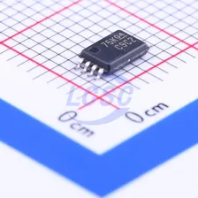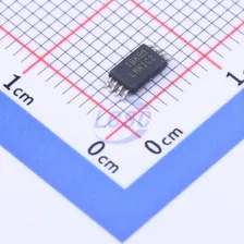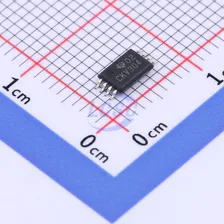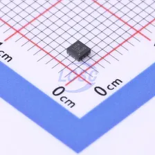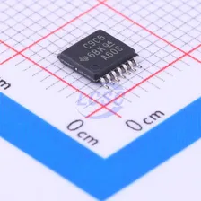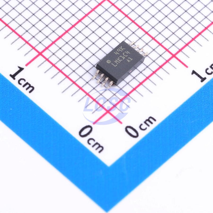
LMK1C1104PWR
250MHz 4 TSSOP-8 Clock Buffers, Drivers RoHS
LVCMOS clock buffer
- Manufacturer
- TI
- Manufacturer part #
- LMK1C1104PWR
- Store part #
- C1855734
- Package / case
- TSSOP-8
- Category
- Clock Buffers, Drivers
- Packaging
- Tape & Reel (TR)
Every Order Guarantee
100% Authentic · 30-Day Return or Replacement · policy
11,847 in stock
#C1855734
Stock & price checked 6 days ago
| Quantity | Unit price | Pack price |
|---|---|---|
| 1+ | ₹166.49 | ₹166.49 |
| 10+ | ₹137.16 | ₹1,371.60 |
| 30+ | ₹121.07 | ₹3,632.10 |
| 100+ | ₹102.59 | ₹10,259.00 |
| 500+ | ₹94.55 | ₹47,275.00 |
| 1,000+ | ₹90.85 | ₹90,850.00 |
1 × ₹166.49
₹166.49
excl. GST
₹196.46 incl. 18% GST
- Dispatch in 7–10 working days
- GST invoice with every order
- Standard pack: 2,000 per reel
LMK1C1104PWR
₹166.49 for 1 + GST
Specifications
- Operating Temperature
- -40℃~+125℃
- Voltage - Supply
- 1.71V;2.375V;1.89V~3.135V;2.625V;3.465V
- Features
- Multi-channel fan-out/isolation drive;Output enable/shutdown
- Number of Inputs
- 1
- Output Frequency(Max)
- 250MHz
- Number of outputs
- 4
Packaging & compliance
- RoHS
- ROHS3 Compliant
- Lifecycle
- Active
- ECCN
- EAR99
- Packaging
- Tape & Reel (TR)
- Standard pack
- 2,000 / Reel
- Sold per
- Piece
- Minimum order
- 1
- Unit weight
- 0.283 g
Overview
High-performance 1:2, 1:3, or 1:4 LVCMOS clock buffers. Three different fan-out options are available: 1:2, 1:3, and 1:4. The entire series is designed using a modular approach. All devices are pin-compatible with each other and backward-compatible with the CDCLVC110x series. All devices in this series feature the same high-performance characteristics, such as low added jitter, low skew, and a wide operating temperature range. They have a synchronous output enable control terminal (1G), which can switch the output to a low-level state when 1G is at a low level. These devices have fail-safe inputs, which prevent the output from oscillating in the absence of an input signal and allow the input signal to be provided before VDD. They can operate at voltages of 1.8V, 2.5V, and 3.3V and can function within a temperature range of –40°C to 125°C.
Applications
- Factory Automation & Control
- Telecom Equipment
- Data Center & Enterprise Computing
- Power Grid Infrastructure
- Motor Drives
- Medical Imaging
Key features
- High-performance 1:2, 1:3, or 1:4 LVCMOS clock buffer
- Ultra-low output skew, <50ps
- Ultra-low additive jitter, max <501fs
- Typical 7.5fs at VDD = 3.3V
- Typical 10fs at VDD = 2.5V
- Typical 19.2fs at VDD = 1.8V
- Ultra-low propagation delay, <3ns
- Synchronous output enable
- Supply voltage: 3.3V, 2.5V, or 1.8V
- 3.3V tolerant input across all supply voltages
- Failsafe input
- fmax = 250MHz (3.3V)
- Δfmax = 200MHz (2.5V and 1.8V)
- Operating temperature range: -40°C to 125°C
- 8-pin TSSOP package
- 8-pin WSON package
Same category