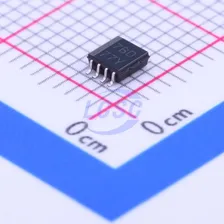
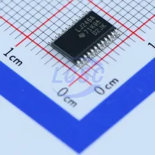
CD40109BPWR
4 1 TSSOP-16 Translators, Level Shifters RoHS
CMOS Quad Low-to-High Voltage Level Shifter
- Manufacturer
- TI
- Manufacturer part #
- CD40109BPWR
- Store part #
- C131950
- Package / case
- TSSOP-16
- Category
- Translators, Level Shifters
- Packaging
- Tape & Reel (TR)
Every Order Guarantee
100% Authentic · 30-Day Return or Replacement · policy
2,146 in stock
#C131950
Stock & price checked 5 days ago
| Quantity | Unit price | Pack price |
|---|---|---|
| 1+ | ₹58.42 | ₹58.42 |
| 10+ | ₹46.12 | ₹461.20 |
| 30+ | ₹40.69 | ₹1,220.70 |
| 100+ | ₹34.19 | ₹3,419.00 |
| 500+ | ₹28.94 | ₹14,470.00 |
| 1,000+ | ₹27.13 | ₹27,130.00 |
1 × ₹58.42
₹58.42
excl. GST
₹68.94 incl. 18% GST
- Dispatch in 7–10 working days
- GST invoice with every order
- Standard pack: 2,000 per reel
CD40109BPWR
₹58.42 for 1 + GST
Specifications
- output type
- Tri-State
- Operating Temperature
- -55℃~+125℃
- Number of Elements
- 4
- Channel Type
- Unidirectional
- Features
- Output enable high-impedance
- Voltage - Supply
- 3V~18V;3V~18V
- Number of Circuits
- 1
Packaging & compliance
- RoHS
- ROHS3 Compliant
- Lifecycle
- Active
- ECCN
- EAR99
- Packaging
- Tape & Reel (TR)
- Standard pack
- 2,000 / Reel
- Sold per
- Piece
- Minimum order
- 1
- Unit weight
- 0.183 g
Overview
CD40109B contains four low-to-high-voltage level-shifting circuits. Each circuit will shift a low-voltage digital-logic input signal (A, B, C, D) with logical 1 = VCC and logical 0 = VSS to a higher-voltage output signal (E, F, G, H) with logical 1 = VDD and logical 0 = VSS. The CD40109, unlike other low- to- high level- shifting circuits, does not require the presence of the high- voltage supply (VDD) before the application of either the low- voltage supply (VCC) or the input signals. There are no restrictions on the sequence of application of VDD, VCC, or the input signals. In addition, with one exception there are no restrictions on the relative magnitudes of the supply voltages or input signals within the device maximum ratings, provided that the input signal swings between VSS and at least 0.7VCC; VCC may exceed VDD, and input signals may exceed VCC and VDD. When operated in the mode VCC > VDD, the CD40109 will operate as a high- to- low level-shifter. The CD40109 also features individual three- state output capability. A low level on any of the separately enabled three- state output controls produces a high- impedance state in the corresponding output. The CD40109B- Series types are supplied in 16- lead ceramic dual- in- line packages (F3A suffix), 16- lead dual- in- line plastic packages (E suffix), 16- lead small- outline packages (NSR suffix), and 16- lead thin shrink small- outline packages (PW and PWR suffixes).
Applications
- High- or- low level- shifting with three- state outputs for unidirectional or bidirectional bussing
- Isolation of logic subsystems using separate power supplies from supply operating, supply loss and supply regulation considerations
Key features
- Independence of power supply sequence considerations - Vcc can exceed VDD, input signals can exceed both VCC and VDD
- Up and down level- shifting capability
- Three- state outputs with separate enable controls
- Standardized, symmetrical output characteristics
- 100% tested for quiescent current at 20V
- Maximum input current of 1μA at 18V over full package- temperature range; 100nA at 18V and 200℃
- Noise margin (full package- temperature range):
- = 1V at VCC = 5V, VDD = 10V
- = 2V at VCC = 10V, VDD = 15V
- 5- V, 10- V, and 15- V parametric ratings
- Meets all requirements of JEDEC Tentative Standard No.13B Standard Specifications for Description of B-Series CMOS Devices
Same category
More in Translators, Level Shifters
TI
SN74AVC4T774RSVR380Mbps 1 4 UQFN-16(1.8x2.6) Translators, Level Shifters RoHS
From
₹64.83
1,11,131 in stock