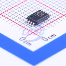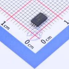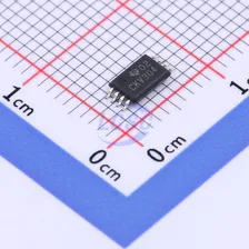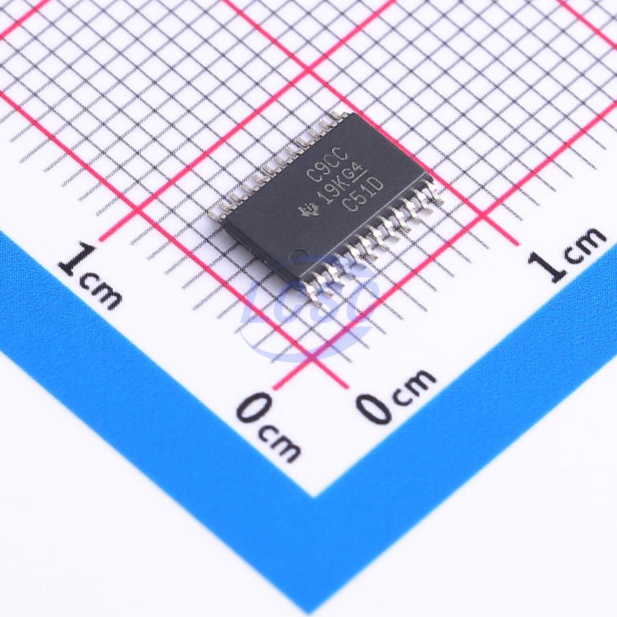
CDCLVC1112PWR
2.3V~3.6V 250MHz 12 TSSOP-24 Clock Buffers, Drivers RoHS
LVCMOS High-Performance Clock Buffer Family
- Manufacturer
- TI
- Manufacturer part #
- CDCLVC1112PWR
- Store part #
- C2876940
- Package / case
- TSSOP-24
- Category
- Clock Buffers, Drivers
- Packaging
- Tape & Reel (TR)
Every Order Guarantee
100% Authentic · 30-Day Return or Replacement · policy
1,982 in stock
#C2876940
Stock & price checked 5 days ago
| Quantity | Unit price | Pack price |
|---|---|---|
| 1+ | ₹744.74 | ₹744.74 |
| 10+ | ₹633.55 | ₹6,335.50 |
| 30+ | ₹567.53 | ₹17,025.90 |
| 100+ | ₹500.85 | ₹50,085.00 |
| 500+ | ₹470.01 | ₹2,35,005.00 |
| 1,000+ | ₹456.10 | ₹4,56,100.00 |
1 × ₹744.74
₹744.74
excl. GST
₹878.79 incl. 18% GST
- Dispatch in 7–10 working days
- GST invoice with every order
- Standard pack: 2,000 per reel
CDCLVC1112PWR
₹744.74 for 1 + GST
Specifications
- Operating Temperature
- -40℃~+85℃
- Voltage - Supply
- 2.3V~3.6V
- Features
- Output enable/shutdown
- Number of Inputs
- 1
- Output Frequency(Max)
- 250MHz
- Number of outputs
- 12
Packaging & compliance
- RoHS
- ROHS3 Compliant
- Lifecycle
- Active
- ECCN
- EAR99
- Packaging
- Tape & Reel (TR)
- Standard pack
- 2,000 / Reel
- Sold per
- Piece
- Minimum order
- 1
- Unit weight
- 0.139 g
Overview
The CDCLVC11xx is a modular, high-performance, low-skew, general-purpose clock buffer family. The entire family is designed with a modular approach in mind. It is intended to round up TI's series of LVCMOS clock generators. Seven different fan-out variations, 1:2 to 1:12, are available. All of the devices are pin-compatible to each other for easy handling. All family members share the same high performing characteristics such as low additive jitter, low skew, and wide operating temperature range. The CDCLVC11xx supports an asynchronous output enable control (1G) which switches the outputs into a low state when 1G is low. The CDCLVC11xx family operates in a 2.5-V and 3.3-V environment and are characterized for operation from -40°C to 85°C.
Applications
- General-Purpose Communication, Industrial, and Consumer Applications
Key features
- High-Performance 1:2, 1:3, 1:4, 1:6, 1:8, 1:10, 1:12 LVCMOS Clock Buffer Family
- Very Low Pin-to-Pin Skew <50 ps
- Very Low Additive Jitter <100 fs
- Supply Voltage: 3.3 V or 2.5 V
- Δfmax = 250 MHz for 3.3 V
- Δfmax = 180 MHz for 2.5 V
- Operating Temperature Range: -40°C to 85°C
- Available in 8-, 14-, 16-, 20-, 24-Pin TSSOP Package (All Pin-Compatible)
Alternatives
Similar parts — check the datasheet before substituting.
| Part | Manufacturer | Package | Stock | Price from (excl. GST) | Action | |
|---|---|---|---|---|---|---|
 | CDCLVC1112PW#C1520139TI · TSSOP-24 | TI | TSSOP-24 | On request | Price on request | Quote |
Same category