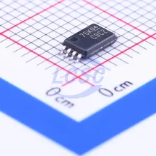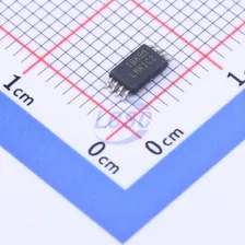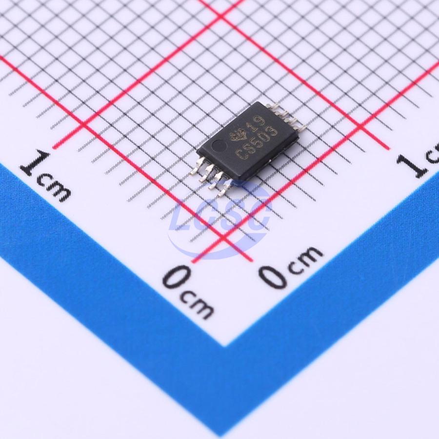
CDCS503PWR
3V~3.6V 108MHz 1 TSSOP-8 Clock Buffers, Drivers RoHS
Clock Buffer/Clock Multiplier With Optional SSC
- Manufacturer
- TI
- Manufacturer part #
- CDCS503PWR
- Store part #
- C2672805
- Package / case
- TSSOP-8
- Category
- Clock Buffers, Drivers
- Packaging
- Tape & Reel (TR)
Every Order Guarantee
100% Authentic · 30-Day Return or Replacement · policy
1,975 in stock
#C2672805
Stock & price checked 25 h ago
| Quantity | Unit price | Pack price |
|---|---|---|
| 1+ | ₹227.52 | ₹227.52 |
| 10+ | ₹192.31 | ₹1,923.10 |
| 30+ | ₹172.97 | ₹5,189.10 |
| 100+ | ₹151.03 | ₹15,103.00 |
| 500+ | ₹141.24 | ₹70,620.00 |
| 1,000+ | ₹136.90 | ₹1,36,900.00 |
1 × ₹227.52
₹227.52
excl. GST
₹268.47 incl. 18% GST
- Dispatch in 7–10 working days
- GST invoice with every order
- Standard pack: 2,000 per reel
CDCS503PWR
₹227.52 for 1 + GST
Specifications
- Operating Temperature
- -40℃~+85℃
- Voltage - Supply
- 3V~3.6V
- Features
- Built-in phase-locked loop;Spread spectrum;Output enable/shutdown
- Number of Inputs
- 1
- Output Frequency(Max)
- 108MHz
- Number of outputs
- 1
Packaging & compliance
- RoHS
- ROHS3 Compliant
- Lifecycle
- Active
- Moisture sensitivity
- MSL 1 (unlimited)
- ECCN
- EAR99
- Packaging
- Tape & Reel (TR)
- Standard pack
- 2,000 / Reel
- Sold per
- Piece
- Minimum order
- 1
- Unit weight
- 0.076 g
Overview
The CDCS503 is a spread spectrum capable, LVCMOS Input Clock Buffer with selectable frequency multiplication. It shares major functionality with the CDCS502 but utilizes a LVCMOS input stage instead of the crystal input stage of the CDCS502. Also an Output Enable pin has been added to the CDCS503. The device accepts a 3.3V LVCMOS signal at the input. The input signal is processed by a PLL, whose output frequency is either equal to the input frequency or multiplied by the factor of 4. The PLL is also able to spread the clock signal by ±0%, ±0.5%, ±1% or ±2% centered around the output clock frequency with a triangular modulation. It can generate output frequencies between 8MHz and 108MHz. A separate control pin can be used to enable or disable the output. The CDCS503 operates in 3.3V environment. It is characterized for operation from -40°C to 85°C, and available in an 8-pin TSSOP package.
Applications
- Consumer and Industrial Applications requiring EMI reduction through Spread Spectrum Clocking and/ or Clock Multiplication
Key features
- Part of a Family of Easy to use Clock Generator Devices With Optional SSC
- Clock Multiplier With Selectable Output Frequency and Selectable SSC
- SSC Controllable via 2 External Pins – ±0%, ±0.5%, ±1%, ±2% Center Spread
- Frequency Multiplication Selectable Between x1 or x4 With One External Control Pin
- Output Disable via Control Pin
- Single 3.3V Device Power Supply
- Wide Temperature Range -40°C to 85°C
- Low Space Consumption by 8 Pin TSSOP Package
Alternatives
Similar parts — check the datasheet before substituting.
| Part | Manufacturer | Package | Stock | Price from (excl. GST) | Action | |
|---|---|---|---|---|---|---|
 | CDCS503TPWRQ1#C553154TI · TSSOP-8 | TI | TSSOP-8 | 21 | ₹204.91 · 21 in stock | View |
 | CDCS504TPWRQ1#C2869422TI · TSSOP-8 | TI | TSSOP-8 | On request | ₹116.79 · 0 in stock | View |
Same category