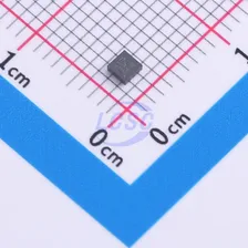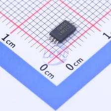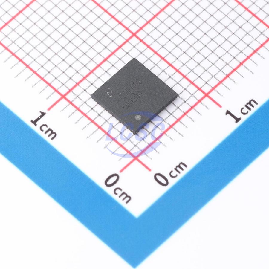
LMK00308SQX/NOPB
3.15V~3.45V 3.1GHz 9 HVQFN-40(6x6) Clock Buffers, Drivers RoHS
3GHz 8-channel output differential clock buffer/level shifter
- Manufacturer
- TI
- Manufacturer part #
- LMK00308SQX/NOPB
- Store part #
- C2673034
- Package / case
- HVQFN-40(6x6)
- Category
- Clock Buffers, Drivers
- Packaging
- Tape & Reel (TR)
Every Order Guarantee
100% Authentic · 30-Day Return or Replacement · policy
2,250 in stock
#C2673034
Stock & price checked 28 h ago
| Quantity | Unit price | Pack price |
|---|---|---|
| 1+ | ₹271.68 | ₹271.68 |
| 10+ | ₹247.39 | ₹2,473.90 |
| 30+ | ₹232.21 | ₹6,966.30 |
| 100+ | ₹216.83 | ₹21,683.00 |
| 500+ | ₹209.67 | ₹1,04,835.00 |
| 1,000+ | ₹206.63 | ₹2,06,630.00 |
1 × ₹271.68
₹271.68
excl. GST
₹320.58 incl. 18% GST
- Dispatch in 7–10 working days
- GST invoice with every order
- Standard pack: 2,500 per reel
LMK00308SQX/NOPB
₹271.68 for 1 + GST
Specifications
- Operating Temperature
- -40℃~+85℃
- Voltage - Supply
- 3.15V~3.45V
- Features
- Multi-channel fan-out/isolation drive;Output enable/shutdown
- Number of Inputs
- 3
- Output Frequency(Max)
- 3.1GHz
- Number of outputs
- 9
Packaging & compliance
- RoHS
- ROHS3 Compliant
- Lifecycle
- Active
- Moisture sensitivity
- MSL 3 (168 hours)
- ECCN
- EAR99
- Packaging
- Tape & Reel (TR)
- Standard pack
- 2,500 / Reel
- Sold per
- Piece
- Minimum order
- 1
- Unit weight
- 0.235 g
Overview
The LMK00308 is an 8-channel output differential fanout buffer operating at 3 GHz, designed for high-frequency, low-jitter clock/data distribution and level conversion. It can select the input clock from two general-purpose inputs or one crystal oscillator input. The selected input clock is distributed to two groups: four differential outputs and one LVCMOS output. The two differential output groups can be independently configured as LVPECL, LVDS, or HCSL drivers, or disabled. The LVCMOS output has a synchronous enable input for glitch-free operation when enabling or disabling. The LMK00308 is powered by a 3.3V core power supply and three independent 3.3V/2.5V output power supplies. The LMK00308 offers high performance, versatility, and power efficiency, making it an ideal choice to replace fixed-output buffer devices while increasing the timing margin in the system. The LMK00308 is an 8-output differential clock fanout buffer with low additive jitter that can operate up to 3.1 GHz. It features a 3:1 input multiplexer with an optional crystal oscillator input, two banks of 4 differential outputs with multi-mode buffers (LVPECL, LVDS, HCSL, or Hi-Z), one LVCMOS output, and 3 independent output buffer supplies. The input selection and output buffer modes are controlled via pin strapping. The device is offered in a 40-pin WQFN package and leverages much of the high-speed, low-noise circuit design employed in the LMK04800 family of clock conditioners. The LMK00308 has a 3.3 V core power supply (VCC) and 3 independent 3.3 V/2.5 V output power supplies (VCCOA, VCCOB, VCCOC). Output supply operation at 2.5 V enables lower power consumption and output-level compatibility with 2.5 V receiver devices. The output levels for LVPECL (VOH, VOL) and LVCMOS (VOH) are referenced to the respective Vcco supply, while the output levels for LVDS and HCSL are relatively constant over the specified Vcco range.
Applications
- Clock distribution and level translation for ADC, DAC, multi-gigabit Ethernet, XAUI, Fibre Channel, SATA/SAS, SONET/SDH, CPRI, and high-frequency backplanes
- Switches, routers, line interface cards, timing cards
- Servers, computing, PCIe 3.0
- Remote radio units and baseband units
Key features
- 3:1 input multiplexer
- Two general-purpose inputs operating up to 3.1GHz, accepting LVPECL, LVDS, CML, SSTL, HSTL, HCSL, or single-ended clock signals
- One crystal input accepting 10 to 40MHz crystal or single-ended enable clock
- 2 banks with 4 differential outputs each
- LVPECL, LVDS, HCSL, or Hi-Z (selectable per bank)
- LMK03806 additive jitter at 156.25MHz clock source: 20fs RMS (10kHz - 1MHz); 51fs RMS (12kHz - 20MHz) for LVPECL
- High PSRR: -65/-76dBc (LVPECL/LVDS) at 156.25MHz
- LVCMOS outputs with synchronous enable drive
- Pin-controlled configuration
- Vcc core supply: 3.3V±5%
- 3 independent Vcco output supplies: 3.3V/2.5V±5%
- Industrial temperature range: -40°C to +85°C
- 40-lead WQFN package (6mm x 6mm)
Same category