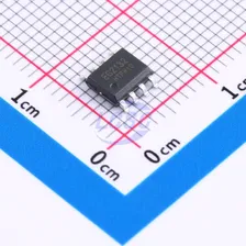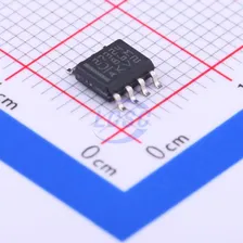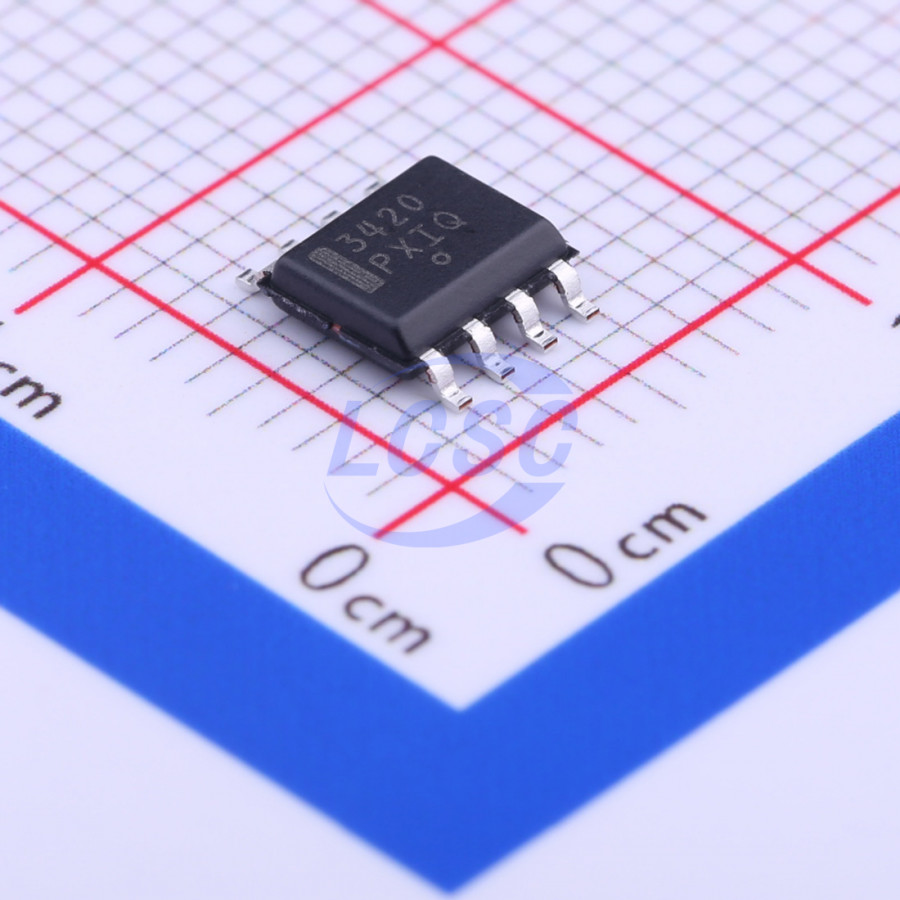
NCP3420DR2G
4.6V~13.2V 2.5A SOIC-8 Gate Drivers RoHS
MOSFET Driver with Dual Outputs for Synchronous Buck Converters
- Manufacturer
- onsemi
- Manufacturer part #
- NCP3420DR2G
- Store part #
- C154600
- Package / case
- SOIC-8
- Category
- Gate Drivers
- Packaging
- Tape & Reel (TR)
Every Order Guarantee
100% Authentic · 30-Day Return or Replacement · policy
7,044 in stock
#C154600
Stock & price checked 6 days ago
| Quantity | Unit price | Pack price |
|---|---|---|
| 1+ | ₹55.17 | ₹55.17 |
| 10+ | ₹42.91 | ₹429.10 |
| 30+ | ₹37.69 | ₹1,130.70 |
| 100+ | ₹31.20 | ₹3,120.00 |
| 500+ | ₹28.30 | ₹14,150.00 |
| 1,000+ | ₹26.51 | ₹26,510.00 |
1 × ₹55.17
₹55.17
excl. GST
₹65.10 incl. 18% GST
- Dispatch in 7–10 working days
- GST invoice with every order
- Standard pack: 2,500 per reel
NCP3420DR2G
₹55.17 for 1 + GST
Specifications
- Low Level Delay Time
- 30ns
- High Level Delay Time
- 30ns
- Voltage - Supply
- 4.6V~13.2V
- Driven Configuration
- Half-Bridge
- Operating Temperature
- 0℃~+85℃
- Current - Output Low(IOL)
- 2.5A
- Rise Time
- 10ns
- Fall Time
- 10ns
- Features
- Enable shutdown;Dead-time control;Interleaved conduction protection
- Load Type
- MOSFET
Packaging & compliance
- RoHS
- ROHS3 Compliant
- Lifecycle
- Active
- ECCN
- EAR99
- Packaging
- Tape & Reel (TR)
- Standard pack
- 2,500 / Reel
- Sold per
- Piece
- Minimum order
- 1
- Unit weight
- 0.22 g
Overview
The NCP3420 is a single Phase 12 V MOSFET gate driver optimized to drive the gates of both high−side and low−side power MOSFETs in a synchronous buck converter. The high−side and low−side driver is capable of driving a 3000 pF load with a 30 ns propagation delay and a 20 ns transition time. With a wide operating voltage range, high or low side MOSFET gate drive voltage can be optimized for the best efficiency. Internal adaptive nonoverlap circuitry further reduces switching losses by preventing simultaneous conduction of both MOSFETs. The floating top driver design can accommodate VBST voltages as high as 35 V, with transient voltages as high as 40 V. Both gate outputs can be driven low by applying a low logic level to the Output Disable (OD) pin. An Undervoltage Lockout function ensures that both driver outputs are low when the supply voltage is low, and a Thermal Shutdown function provides the IC with overtemperature protection.
Applications
- High current multi−phase buck regulators that convert 12 V rail directly to the core voltage required by complex logic chips
Key features
- Thermal Shutdown for System Protection
- Internal Pulldown Resistor Suppresses Transient Turn On of Either MOSFET
- Anti Cross−Conduction Protection Circuitry
- One Input Signal Controls Both the Upper and Lower Gate Outputs
- Output Disable Control Turns Off Both MOSFETs
- Complies with VRM10.x and VRM11.x Specifications
- Undervoltage Lockout
- Thermally Enhanced Package Available
- These are Pb−Free Devices
Same category