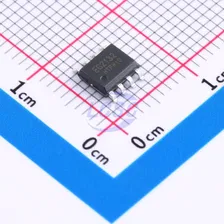
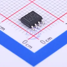
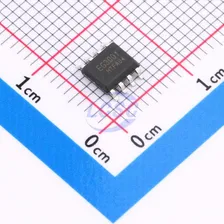
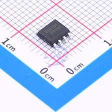
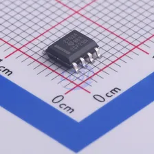
NSG27712
10V~20V 5A 4.5A SOP-8 Gate Drivers
- Manufacturer
- WXNSIC
- Manufacturer part #
- NSG27712
- Store part #
- C52975934
- Package / case
- SOP-8
- Category
- Gate Drivers
- Packaging
- Tape & Reel (TR)
Every Order Guarantee
100% Authentic · 30-Day Return or Replacement · policy
1,485 in stock
#C52975934
Stock & price checked 5 days ago
| Quantity | Unit price | Pack price |
|---|---|---|
| 5+ | ₹35.96 | ₹179.80 |
| 50+ | ₹28.15 | ₹1,407.50 |
| 150+ | ₹24.81 | ₹3,721.50 |
| 500+ | ₹20.64 | ₹10,320.00 |
| 2,500+ | ₹18.77 | ₹46,925.00 |
| 4,000+ | ₹17.66 | ₹70,640.00 |
5 × ₹35.96
₹179.80
excl. GST
₹212.16 incl. 18% GST
- Dispatch in 7–10 working days
- GST invoice with every order
- Standard pack: 4,000 per reel
NSG27712
₹179.80 for 5 + GST
Specifications
- Input Logic Level - Low
- 800mV~1.5V
- Quiescent Current
- 240uA
- Input Logic Level - High
- 2.2V~2.6V
- Voltage - Supply
- 10V~20V
- Operating Temperature
- -40℃~+125℃
- Driven Configuration
- High Side;Low Side
- Current - Output Low(IOL)
- 5A
- Rise Time
- 15ns
- Fall Time
- 9ns
- Features
- Dead-time control;Interleaved conduction protection
- Current - Output High(IOH)
- 4.5A
- Load Type
- MOSFET;IGBT
Packaging & compliance
- RoHS
- RoHS
- Lifecycle
- Active
- Packaging
- Tape & Reel (TR)
- Standard pack
- 4,000 / Reel
- Sold per
- Piece
- Minimum order
- 5 (multiples of 5)
- Unit weight
- 0.366 g
Overview
The NSG27712 is a 700V high-side and low-side gate driver with 4.5A source and 5A sink current capability, designed to drive power MOSFETs or IGBTs. For IGBTs, the recommended VCC operating voltage range is 10V to 20V; for power MOSFETs, the recommended VCC operating voltage range is 10V to 17V. The device integrates protection features that hold the output low when the input remains open or the minimum input pulse width specification is not met. Its interlock and dead-time function prevents both outputs from conducting simultaneously. Additionally, the device supports a wide bias supply range and provides UVLO protection for VCC and VB bias supplies. Built on advanced high-voltage process technology, it offers robust drive capability and superior noise and transient immunity, including large input negative voltage tolerance, high dV/dt immunity, and a wide negative transient SOA at the switching node. The device contains one ground-referenced channel and one floating channel, the latter designed for bootstrap or isolated supply operation. It features fast propagation delay and excellent channel-to-channel delay matching. Each channel is independently controlled by its respective input pins HIN and LIN.
Applications
- Motor drives
- Bridge converters in offline AC/DC power supplies
- High-density switch-mode power supplies for server, telecom, IT, and industrial infrastructure
- DC-to-AC inverters
Key features
- High-side and low-side configurations
- Dual inputs with output interlock and 300ns dead time
- Fully operational up to 680V, with VB pin rated up to 700V
- Recommended VCC operating voltage range: 10V to 20V
- Peak output current: 5.0A sink, 4.5A source
- 50V/ns dV/dt immunity
- Logic operation on VS pin up to -11V
- Input negative voltage tolerance: -10V
- Wide negative transient safe operating area
- Under-voltage lockout protection for both channels
- Matched propagation delay (typical 20ns)
- Floating channel designed for bootstrap operation
- Low quiescent current
- TTL and CMOS compatible inputs
- Industry-standard SOP-8 package
- All parameters rated over -40°C to +125°C temperature range
Same category