AWINIC(Shanghai Awinic Tech)
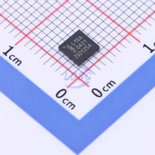
AW9523BTQR16 I2C TQFN-24-EP(4x4) I/O Expanders RoHS
From
₹46.24
76,390 in stock
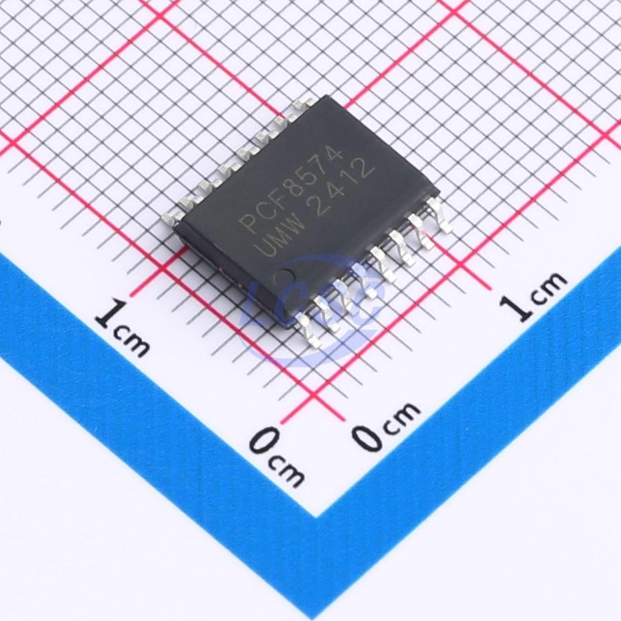
8 I2C SOIC-16-300mil I/O Expanders RoHS
8-Bit I/O Expander for I²C Bus
Every Order Guarantee
100% Authentic · 30-Day Return or Replacement · policy
4,815 in stock
#C22396383
Stock & price checked 6 days ago
| Quantity | Unit price | Pack price |
|---|---|---|
| 1+ | ₹79.26 | ₹79.26 |
| 10+ | ₹62.29 | ₹622.90 |
| 30+ | ₹53.91 | ₹1,617.30 |
| 100+ | ₹45.54 | ₹4,554.00 |
| 500+ | ₹40.38 | ₹20,190.00 |
| 1,500+ | ₹37.81 | ₹56,715.00 |
1 × ₹79.26
₹79.26
excl. GST
₹93.53 incl. 18% GST
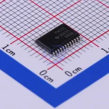
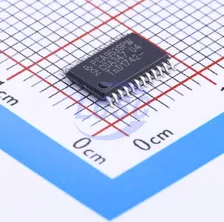
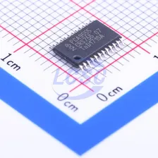
PCF8574DWR(UMW)
₹79.26 for 1 + GST
PCF8574 is primarily used for expanding GPIO ports. Port data is transmitted via the standard two-wire I²C protocol. PCF8574 features 8-bit quasi-bidirectional GPIO ports (P0~P7) capable of directly driving LEDs. Each quasi-bidirectional GPIO port can be used as either an input or output without requiring a data direction control signal. Upon power-up, all GPIO ports are initialized to a high level. The simplified circuit of a GPIO consists of a weak pull-up current path (100μA) and a strong pull-down current path (25mA). This structure allows the port to function as either an input or output without any direction control signal. When used as an input, the port must be written with a logic 1. When a logic 0 is written to an I/O port via the I²C interface, transistor Q2 turns on while Q1 and Q3 turn off. The pull-down path is then activated, providing sufficient sink current to drive an LED. When a logic 1 is written to an I/O port via the I²C interface, transistor Q2 turns off while Q1 and Q3 turn on. Q3 serves as an additional strong current path (1mA) to provide fast rising edges when driving heavy loads. Transistor Q3 conducts only during the Ack period of an I²C write sequence. I²C/SMBus is a two-wire serial communication interface supporting multiple masters and multiple slaves. The device that initiates communication is called the master, and the devices controlled by the master are called slaves. The master is responsible for generating the serial clock (SCL) and controlling bus access. Data transfer is followed by an acknowledge bit after every eight clock pulses. During data transfer, SDA must remain stable while SCL is high, as any change on SDA while SCL is high is interpreted as a START or STOP condition. PCF8574 has 3 hardware address pins (A2/A1/A0), allowing users to select the chip's slave address. The logic levels of these pins must remain unchanged throughout communication; otherwise, communication failure may occur. The address pins must be connected to VCC or GND and must not be left floating, as this will cause communication failure and the chip's standby current will exceed 1μA. The slave address byte consists of 7 address bits and 1 read/write flag bit. The read/write flag bit indicates the direction of data transfer. 0b indicates a write operation; 1b indicates a read operation. Data transmission begins with the MSB of each byte. GPIO output is achieved by writing data to PCF8574. Starting with the slave address byte with the R̄/W̄ bit low, each subsequent byte represents the data to be output to the GPIO ports. PCF8574 latches the received data byte to the GPIO ports on the rising edge of SCL during the Ack bit of each data byte, and samples the GPIO ports on the immediately following falling edge of SCL to ensure that the written data does not trigger an interrupt signal. GPIO input is achieved by reading data from PCF8574. Starting with the slave address byte with the R/W bit high, each subsequent byte represents data sampled from the GPIO ports. PCF8574 samples the GPIO ports on the rising edge of SCL during the Ack bit of the address byte and each data byte, thereby clearing the interrupt signal. Note that when the master sends a NAck bit, PCF8574 does not sample the GPIO ports, and therefore the interrupt signal will not be cleared. If the master sends a high-speed mode code (0000 1xxxb) after a START condition, the chip will not respond to that byte but will switch the input and output filters on the SDA and SCL pins to high-speed mode, allowing the bus to transfer data at communication frequencies up to 2MHz. The chip will continue operating in high-speed mode until a STOP condition appears on the bus. Once a STOP condition is received, the chip will switch the input and output filters back to normal mode.
Same category
AWINIC(Shanghai Awinic Tech)
AW9523BTQR16 I2C TQFN-24-EP(4x4) I/O Expanders RoHS
From
₹46.24
76,390 in stock