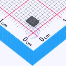
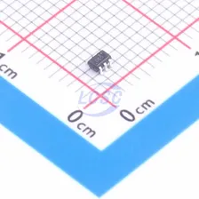
SN74ALVTH16374DLR
8 2 3.2ns@3.3V,50pF SSOP-48-300mil Flip Flops RoHS
16-bit Edge-Triggered D-Type Flip-Flops with 3-State Outputs
- Manufacturer
- TI
- Manufacturer part #
- SN74ALVTH16374DLR
- Store part #
- C2868846
- Package / case
- SSOP-48-300mil
- Category
- Flip Flops
- Packaging
- Tape & Reel (TR)
Every Order Guarantee
100% Authentic · 30-Day Return or Replacement · policy
1,928 in stock
#C2868846
Stock & price checked 5 days ago
| Quantity | Unit price | Pack price |
|---|---|---|
| 1+ | ₹242.31 | ₹242.31 |
| 10+ | ₹203.44 | ₹2,034.40 |
| 30+ | ₹179.03 | ₹5,370.90 |
| 100+ | ₹154.20 | ₹15,420.00 |
| 500+ | ₹142.96 | ₹71,480.00 |
| 1,000+ | ₹138.00 | ₹1,38,000.00 |
1 × ₹242.31
₹242.31
excl. GST
₹285.93 incl. 18% GST
- Dispatch in 7–10 working days
- GST invoice with every order
- Standard pack: 1,000 per reel
SN74ALVTH16374DLR
₹242.31 for 1 + GST
Specifications
- Voltage - Supply
- 2.3V~2.7V;3V~3.6V
- Number of Bits per Element
- 8
- Output Type
- Tri-State
- Operating Temperature
- -40℃~+85℃
- Series
- 74ALVTH Series
- Number of Elements
- 2
- Current - Output High(IOH)
- 8mA
- Current - Output Low(IOL)
- 32mA
- Setup Time
- 1ns;1.5ns
- Quiescent Current
- 100uA
- Hold Time
- 500ps;1ns
- Propagation Delay
- 3.2ns@3.3V,50pF
- Trigger Type
- Rising Edge
Packaging & compliance
- RoHS
- ROHS Compliant
- Lifecycle
- Active
- ECCN
- EAR99
- Packaging
- Tape & Reel (TR)
- Standard pack
- 1,000 / Reel
- Sold per
- Piece
- Minimum order
- 1
- Unit weight
- 1.043 g
Overview
The 'ALVTH16374 devices are 16-bit edge-triggered D-type flip-flops with 3-state outputs designed for 2.5-V or 3.3-V VCC operation, but with the capability to provide a TTL interface to a 5-V system environment. These devices are particularly suitable for implementing buffer registers, I/O ports, bidirectional bus drivers, and working registers. These devices can be used as two 8-bit flip-flops or one 16-bit flip-flop. On the positive transition of the clock (CLK), the flip-flops store the logic levels set up at the data (D) inputs. A buffered output-enable (OE(overline)) input can be used to place the eight outputs in either a normal logic state (high or low logic levels) or a high-impedance state. In the high-impedance state, the outputs neither load nor drive the bus lines significantly. The high-impedance state and the increased drive provide the capability to drive bus lines without need for interface or pullup components. OE does not affect internal operations of the flip-flop. Old data can be retained or new data can be entered while the outputs are in the high-impedance state. Active bus-hold circuitry is provided to hold unused or floating data inputs at a valid logic level. When VCC is between 0 and 1.2 V, the device is in the high-impedance state during power up or power down. However, to ensure the high-impedance state above 1.2 V, OE should be tied to VCC through a pullup resistor; the minimum value of the resistor is determined by the current-sinking capability of the driver. The SN74ALVTH16374 is characterized for operation from -40℃ to 85℃.
Applications
- Buffer registers
- I/O ports
- Bidirectional bus drivers
- Working registers
Key features
- State-of-the-Art Advanced BiCMOS Technology (ABT) Widebus Design for 2.5-V and 3.3-V Operation and Low Static Power Dissipation
- Support Mixed-Mode Signal Operation (5-V Input and Output Voltages With 2.3-V to 3.6-V VCC)
- Typical VOLP (Output Ground Bounce) < 0.8 V at VCC = 3.3V, TA = 25℃
- High Drive (-24/24 mA at 2.5-V VCC and –32/64 mA at 3.3-V)
- Power Off Disables Outputs, Permitting Live Insertion
- High-Impedance State During Power Up and Power Down Prevents Driver Conflict
- Uses Bus Hold on Data Inputs in Place of External Pullup/Pulldown Resistors to Prevent the Bus From Floating
- Auto3-State Eliminates Bus Current Loading When Output Exceeds VCC + 0.5 V
- Latch-Up Performance Exceeds ±50 mA Per JESD 17
- ESD Protection – Exceeds 2000 V Per MIL-STD-883, Method 3015 – Exceeds 200 V Using Machine Model Exceeds 1000 V Using Charged-Device Model, Robotic Method
- Flow-Through Architecture Facilitates Printed Circuit Board Layout
- Distributed VCC and GND Pin Configuration Minimizes High-Speed Switching Noise
- Package Options Include Plastic Shrink Small-Outline (DL), Thin Shrink Small-Outline (DGG), Thin Very Small-Outline (DGV) Packages, and 380-mil Fine-Pitch Ceramic Flat (WD) Package
Same category
More in Flip Flops
Nexperia
74HC574D,6532V~6V 8 1 17ns@4.5V,50pF SOIC-20-300mil Flip Flops RoHS
From
₹42.20
48,155 in stock