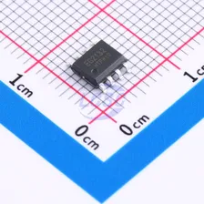
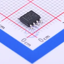
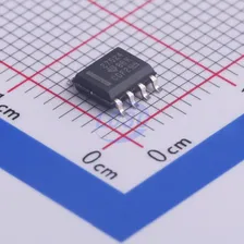
UCC27524DGNR
Low Side Gate Driver IC MOSFET IGBT TSSOP-8-EP-3.0mm
Dual 5A high-speed low-side gate driver
- Manufacturer
- TI
- Manufacturer part #
- UCC27524DGNR
- Store part #
- C130088
- Package / case
- TSSOP-8-EP-3.0mm
- Category
- Gate Drivers
- Packaging
- Tape & Reel (TR)
Every Order Guarantee
100% Authentic · 30-Day Return or Replacement · policy
1,072 in stock
#C130088
Stock & price checked 4 days ago
| Quantity | Unit price | Pack price |
|---|---|---|
| 1+ | ₹166.44 | ₹166.44 |
| 10+ | ₹143.84 | ₹1,438.40 |
| 30+ | ₹131.53 | ₹3,945.90 |
| 100+ | ₹117.41 | ₹11,741.00 |
| 500+ | ₹111.27 | ₹55,635.00 |
| 1,000+ | ₹108.37 | ₹1,08,370.00 |
1 × ₹166.44
₹166.44
excl. GST
₹196.40 incl. 18% GST
- Dispatch in 7–10 working days
- GST invoice with every order
- Standard pack: 2,500 per reel
UCC27524DGNR
₹166.44 for 1 + GST
Specifications
- Input Logic Level - Low
- 1V~1.4V
- Quiescent Current
- 75uA
- Input Logic Level - High
- 1.9V~2.3V
- Voltage - Supply
- 4.5V~18V
- Operating Temperature
- -40℃~+140℃
- Driven Configuration
- Low Side
- Current - Output Low(IOL)
- 5A
- Rise Time
- 7ns
- Fall Time
- 6ns
- Features
- Enable shutdown
- Current - Output High(IOH)
- 5A
- Load Type
- MOSFET;IGBT
Packaging & compliance
- RoHS
- ROHS3 Compliant
- Lifecycle
- Active
- ECCN
- EAR99
- Packaging
- Tape & Reel (TR)
- Standard pack
- 2,500 / Reel
- Sold per
- Piece
- Minimum order
- 1
- Unit weight
- 0.205 g
Overview
The UCC2752x family of devices are dual-channel, high-speed, low-side gate drivers capable of effectively driving MOSFET and IGBT power switches. Using a design that substantially reduces shoot-through current internally, the UCC2752x can deliver high peak current pulses of up to 5A source and 5A sink to capacitive loads. The device also features rail-to-rail drive capability and a typical propagation delay as low as 13ns. In addition, the driver features matched internal propagation delays between the two channels, making it well suited for applications with stringent timing requirements for dual gate drives, such as synchronous rectifiers. This also allows the two channels to be paralleled to effectively increase current drive capability, or to drive two switches connected in parallel using a single input signal. The input pin thresholds are based on TTL and CMOS compatible low-voltage logic, which is fixed and independent of the VDD supply voltage. Wide hysteresis between the high and low thresholds provides excellent noise immunity. The UCC2752x family offers a combination of three standard logic options — dual inverting, dual non-inverting, and one inverting plus one non-inverting driver. The UCC27526 features a dual-input design that provides flexibility for both inverting (IN− pin) and non-inverting (IN+ pin) configurations for each channel. Either the IN+ or IN− pin controls the driver output state. Unused input pins can be used for enable and disable functionality. As a safety measure, internal pull-up and pull-down resistors on the input pins of all devices in the UCC2752x family ensure the output remains low when the input pins are left floating. For better control over driver application operation, the UCC27323, UCC27324, and UCC27325 each feature an enable pin (ENA and ENB). For active-high logic, these pins are internally pulled up to VDD and can be left open for standard operation.
Applications
- Switch-mode power supplies
- DC-to-DC converters
- Motor control, solar
- Gate drivers for emerging wide-bandgap power devices such as GaN
Key features
- Industry-standard pinout
- Two independent gate drive channels
- 5A peak source and sink drive current
- Independent enable function per output
- TTL and CMOS compatible logic thresholds independent of supply voltage
- Hysteretic logic thresholds for high noise immunity
- Input and enable pin voltage levels not limited by VDD pin bias supply voltage
- 4.5V to 18V single-supply range
- Outputs held low during VDD UVLO (ensuring glitch-free pulse operation during power-up and power-down)
- Fast propagation delay (13ns typical)
- Fast rise and fall times (7ns and 6ns typical)
- 1ns typical delay matching between two channels
- Two outputs parallelable for higher drive current
- Outputs held low when inputs are floating
- PDIP-8, SOIC-8, MSOP-8 packages
- PowerPAD and 3mm x 3mm WSON-8 package options
- -40°C to 140°C operating temperature range
Alternatives
Similar parts — check the datasheet before substituting.
| Part | Manufacturer | Package | Stock | Price from (excl. GST) | Action | |
|---|---|---|---|---|---|---|
| UCC27524DGN#C1549481TI · HVSSOP-8-EP-0.65mm | TI | HVSSOP-8-EP-0.65mm | On request | Price on request | Quote | |
Same category