JSMSEMI
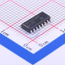
74HC595D2V~6V 1 15ns@6V,50pF Serial-to-Serial or Parallel SOP-16 Shift Registers RoHS
From
₹8.83
3,36,720 in stock
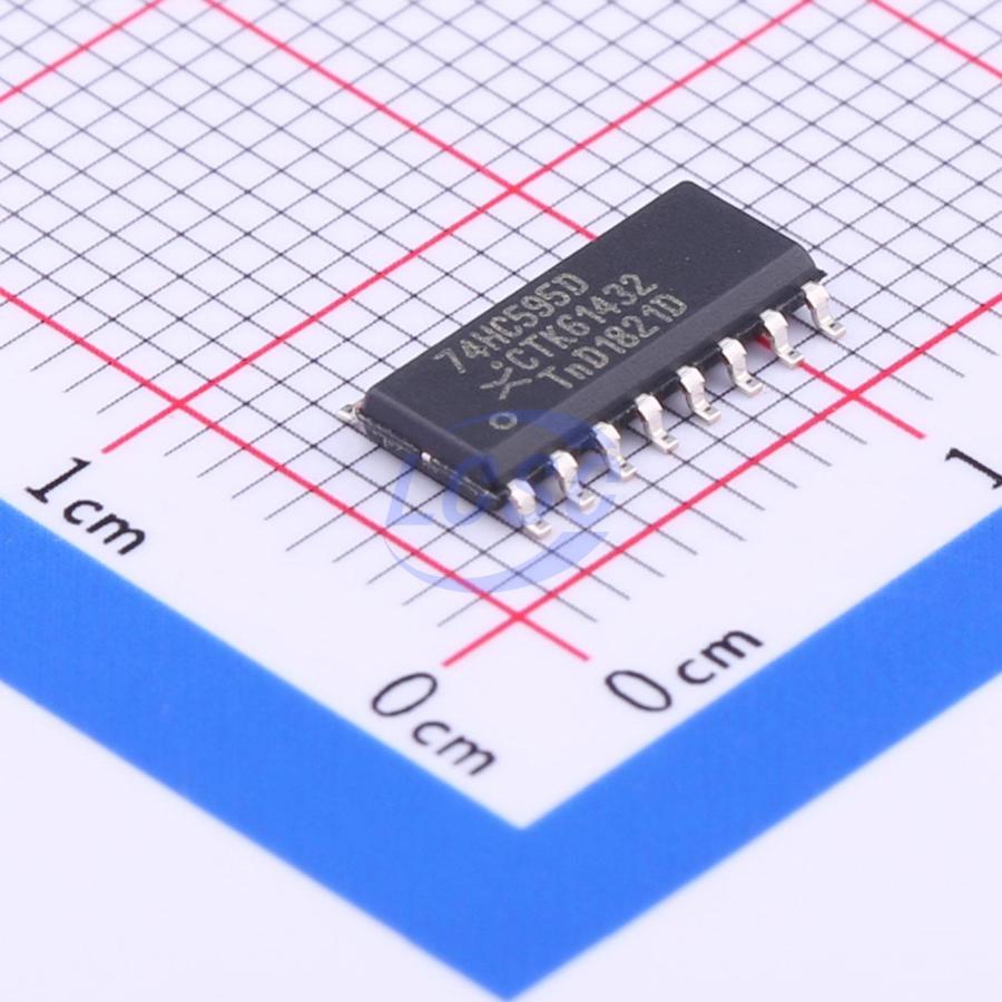
2V~6V 1 19ns@4.5V,50pF Serial-to-Serial or Parallel SOIC-16 Shift Registers RoHS
8-bit serial-in, serial or parallel-out shift register with output latches; 3-state
Every Order Guarantee
100% Authentic · 30-Day Return or Replacement · policy
2,91,275 in stock
#C5947
Stock & price checked 6 days ago
| Quantity | Unit price | Pack price |
|---|---|---|
| 5+ | ₹12.80 | ₹64.00 |
| 50+ | ₹10.16 | ₹508.00 |
| 150+ | ₹8.81 | ₹1,321.50 |
| 500+ | ₹7.70 | ₹3,850.00 |
| 2,500+ | ₹7.30 | ₹18,250.00 |
| 5,000+ | ₹7.04 | ₹35,200.00 |
5 × ₹12.80
₹64.00
excl. GST
₹75.52 incl. 18% GST
74HC595D,118
₹64.00 for 5 + GST
The 74HC595; 74HCT595 is an 8-bit serial-in/serial or parallel-out shift register with a storage register and 3-state outputs. Both the shift and storage register have separate clocks. The device features a serial input (DS) and a serial output (Q7S) to enable cascading and an asynchronous reset MR input. A LOW on MR will reset the shift register. Data is shifted on the LOW-to-HIGH transitions of the SHCP input. The data in the shift register is transferred to the storage register on a LOW-to-HIGH transition of the STCP input. If both clocks are connected together, the shift register will always be one clock pulse ahead of the storage register. Data in the storage register appears at the output whenever the output enable input (OE) is LOW. A HIGH on OE causes the outputs to assume a high-impedance OFF-state. Operation of the OE input does not affect the state of the registers. Inputs include clamp diodes. This enables the use of current limiting resistors to interface inputs to voltages in excess of VCC.
Similar parts — check the datasheet before substituting.
| Part | Manufacturer | Package | Stock | Price from (excl. GST) | Action | |
|---|---|---|---|---|---|---|
 | 74HC595D-Q100,118#C547127Nexperia · SO-16 | Nexperia | SO-16 | 2,480 | ₹28.77 · 2,480 in stock | View |
 | 74HC595D(MS)#C20538884MSKSEMI · SOP-16 | MSKSEMI | SOP-16 | 440 | ₹8.47 · 440 in stock | View |
 | 74HC595D(XBLW)#C20612517XBLW · SOP-16 | XBLW | SOP-16 | 56,440 | ₹6.91 · 56,440 in stock | View |
 | HT74HC595ARZ#C2895054HTCSEMI · SOIC-16 | HTCSEMI | SOIC-16 | 1,390 | ₹19.06 · 1,390 in stock | View |
 | GM74HC595DR#C49329007GREENMICRO · SOP-16 | GREENMICRO | SOP-16 | 5,945 | ₹11.78 · 5,945 in stock | View |
The 74HC595D is a high-speed CMOS 8-bit serial-in/serial or parallel-out shift register with an internal 8-bit storage register and 3-state parallel outputs (Q0–Q7). Data is shifted into the shift register on the LOW-to-HIGH transition of the shift register clock (SHCP), while data is transferred to the storage register on the LOW-to-HIGH transition of the storage register clock (STCP). An active-LOW Output Enable (OE) places the parallel outputs in a high-impedance OFF-state without affecting the register contents, and an active-LOW Master Reset (MR) asynchronously clears the shift register.
The 74HC595D belongs to Nexperia's 74HC high-speed CMOS logic family and operates over a supply voltage (VCC) range of 2.0 V to 6.0 V with CMOS input logic levels. According to the dynamic characteristics, the device supports a typical maximum operating frequency (fmax) of 91 MHz at VCC = 4.5 V and 108 MHz at VCC = 6.0 V. Table 7 also specifies minimum fmax values of 20 MHz at VCC = 4.5 V and 24 MHz at VCC = 6.0 V over the full −40°C to +125°C operating temperature range. The 3-state parallel outputs can source or sink up to ±6 mA at VCC = 4.5 V.
The 74HC595D is supplied in Nexperia's SOT109-1 (SO16) plastic small-outline package with 16 leads and a 3.9 mm body width. The package has a nominal 1.27 mm (50 mil) lead pitch, a body length of 9.8 mm to 10.0 mm, and a maximum package height of 1.75 mm, making it suitable for standard SO16 PCB footprints.
The ordering code 74HC595D identifies a member of Nexperia's 74HC high-speed CMOS logic family. The device is an 8-bit serial-in/serial or parallel-out shift register with a storage register and 3-state outputs, and the "D" suffix denotes the SO16 (SOT109-1) plastic small-outline package.
The 74HC595D is specified for operation over an ambient temperature range of −40°C to +125°C. The device provides HBM ESD protection exceeding 2,000 V (ANSI/ESDA/JEDEC JS-001 Class 2) and CDM protection exceeding 1,000 V (ANSI/ESDA/JEDEC JS-002 Class C3). The datasheet also notes that the inputs include clamp diodes, enabling the use of current-limiting resistors when interfacing inputs to voltages above VCC.
Same category
JSMSEMI
74HC595D2V~6V 1 15ns@6V,50pF Serial-to-Serial or Parallel SOP-16 Shift Registers RoHS
From
₹8.83
3,36,720 in stock
TI
SN74HC595DR2V~6V 1 6mA 26ns@6V,50pF Serial-to-Serial or Parallel SOIC-16 Shift Registers RoHS
From
₹19.81
2,98,335 in stock
Nexperia
74HC165D,6532V~6V 1 25mA 28ns@6V,50pF Parallel or Serial to Serial SOIC-16 Shift Registers RoHS
From
₹12.63
2,67,140 in stock
Nexperia
74HC595PW,1182V~6V 1 35mA 19ns@4.5V,50pF Serial-to-Serial or Parallel TSSOP-16 Shift Registers RoHS
From
₹12.25
1,97,375 in stock
FM
74HC595D.3V~5V 75mA 22ns@5V,15pF Serial-to-Parallel SOP-16 Shift Registers RoHS
From
₹11.53
1,94,160 in stock
Nexperia
74HC164D,6532V~6V 1 25mA 43ns@6V,50pF Serial-to-Parallel SOIC-14 Shift Registers RoHS
From
₹11.85
1,81,625 in stock