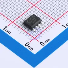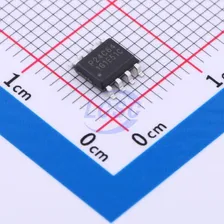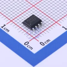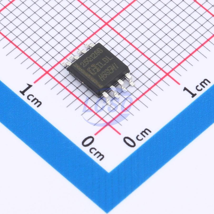
HG25Q128BMW/TR
128Mbit 2.7V~3.6V 133MHz SPI SOP-8-208mil Memory
CMOS Serial Multi I/O Flash Memory
Every Order Guarantee
100% Authentic · 30-Day Return or Replacement · policy
3,269 in stock
#C22461597
Stock & price checked 3 days ago
| Quantity | Unit price | Pack price |
|---|---|---|
| 1+ | ₹179.49 | ₹179.49 |
| 10+ | ₹147.33 | ₹1,473.30 |
| 30+ | ₹129.73 | ₹3,891.90 |
| 100+ | ₹109.95 | ₹10,995.00 |
| 500+ | ₹101.05 | ₹50,525.00 |
| 1,000+ | ₹96.92 | ₹96,920.00 |
1 × ₹179.49
₹179.49
excl. GST
₹211.80 incl. 18% GST
- Dispatch in 15-18 working days
- GST invoice with every order
- Standard pack: 2,500 per reel
HG25Q128BMW/TR
₹179.49 for 1 + GST
Specifications
- Features
- Write enable latch;Hardware write protection;Software write protection;Absolute write protection
- Memory Size
- 128Mbit
- Voltage - Supply
- 2.7V~3.6V
- Program / Erase Cycles
- 100,000 cycles
- Clock Frequency
- 133MHz
- Data Retention - TDR (Year)
- 20 Years
- Block Erase Time(tBE)
- 180ms@(32KB)
- Page Programming Time (Tpp)
- 250us
- Interface
- SPI
Packaging & compliance
- RoHS
- RoHS
- Lifecycle
- Active
- Moisture sensitivity
- MSL 3 (168 hours)
- Packaging
- Tape & Reel (TR)
- Standard pack
- 2,500 / Reel
- Sold per
- Piece
- Minimum order
- 1
- Unit weight
- 0.349 g
Overview
HG25Q128B is 128Mb bits Serial NOR Flash memory, which is configured as 16,777,216x8 internally. When it is in two or four I/O mode, the structure becomes 67,108,864 bits x 2 or 33,554,432 bits x 4. HG25Q128B features a serial peripheral interface and software protocol allowing operation on a simple 3 - wire bus while it is in single I/O mode. The three bus signals are a clock input (SCLK), a serial data input (SI), and a serial data output (SO). Serial access to the device is enabled by CS# input. When it is in two I/O read mode, the SI pin and SO pin become SIO0 pin and SIO1 pin for address/dummy bits input and data output. When it is in four I/O read mode, the SI pin, SO pin, WP# and RESET# pin (of the 8 - pin packages) become SIO0 pin, SIO1 pin, SIO2 pin and SIO3 pin for address/dummy bits input and data output. XSMIO® (Serial Multi I/O) provides sequential read operation on After program/erase command is issued, auto program/erase algorithms which program/erase and verify the specified page or sector/block locations will be executed. Program command is executed on byte basis, or page (256 bytes) basis, or word basis. Erase command is executed on 4K - byte sector, 32K - byte block, or 64K - byte block, or whole chip basis. To provide user with ease of interface, a status register is included to indicate the status of the chip. The status read command can be issued to detect completion status of a program or erase operation via WIP bit. Advanced security features enhance the protection and security functions. The HG25Q128B utilizes proprietary memory cell, which reliably stores memory contents even after 100,000 program and erase cycles.
Key features
- GENERAL
- Supports Serial Peripheral Interface -- Mode 0 and Mode 3
- Single Power Supply Operation - 2.7 to 3.6 volts for read, erase, and program operations
- 134,217,728x1 bit structure or 67,108,864x2 bits (two I/O mode) structure or 33,554,432x4 bits (four I/O mode) structure
- Protocol Support - Single I/O, Dual I/O and Quad I/O
- Latch - up protected to 100mA from - 1V to Vcc + 1V
- Low Vcc write inhibit is from 1.5V to 2.5V
- Fast read for SPI mode - Supports clock frequency up to 133MHz for all protocols - Supports Fast Read, 2READ, DREAD, 4READ, QREAD instructions - Supports DTR (Double Transfer Rate) Mode - Configurable dummy cycle number for fast read operation
- Supports Performance Enhance Mode - XIP (execute - in - place)
- Quad Peripheral Interface (QPI) available Equal 4K byte sectors, or Equal Blocks with 32K bytes or 64K bytes each - Any Block can be erased individually Programming: - 256byte page buffer - Quad Input/Output page program(4PP) to enhance program performance
- Typical 100,000 erase/program cycles
- 20 years data retention
- SOFTWARE FEATURES
- Input Data Format - 1 - byte Command code
- Advanced Security Features - Block lock protection The BP0 - BP3 and T/B status bits define the size of the area to be protected against program and erase instructions - Individual sector protection function (Solid Protect) Additional 4K bit security OTP - Features unique identifier - Factory locked identifiable, and customer lockable
- Command Reset
- Program/Erase Suspend and Resume operation
- Electronic Identification - JEDEC 1 - byte manufacturer ID and 2 - byte device ID - RES command for 1 - byte Device ID - REMS command for 1 - byte manufacturer ID and 1 - byte device ID
- Supports Serial Flash Discoverable Parameters (SFDP) mode
- HARDWARE FEATURES
- SCLK Input - Serial clock input
- SI/SIO0 - Serial Data Input or Serial Data Input/Output for 2xI/O read mode and 4xI/O read mode
- SO/SIO1 - Serial Data Output or Serial Data Input/Output for 2xI/O read mode and 4xI/O read mode
- WP#/SIO2 - Hardware Write Protection or Serial Data Input/ Output for 4xI/O read mode
- NC/SIO3 - No connection or Serial Data Input/Output for 4xI/O read mode
- RESET# - Hardware Reset pin
- RESET#/SIO3 - Hardware Reset pin or Serial Data Input/Output for 4xI/O read mode
- PACKAGE - 8 - pins SOP (208mil)
- All devices are RoHS Compliant and Halogen free
Same category