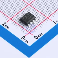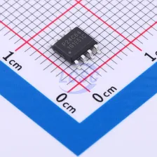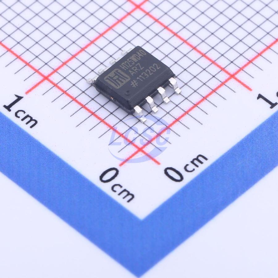
HT25WD40ARZ
4Mbit 1.65V~3.6V 100MHz SPI SOP-8 Memory
SERIAL NOR FLASH WITH DUAL SPI
Every Order Guarantee
100% Authentic · 30-Day Return or Replacement · policy
878 in stock
#C2928800
Stock & price checked 45 h ago
| Quantity | Unit price | Pack price |
|---|---|---|
| 1+ | ₹33.49 | ₹33.49 |
| 10+ | ₹26.37 | ₹263.70 |
| 30+ | ₹23.31 | ₹699.30 |
| 100+ | ₹19.50 | ₹1,950.00 |
| 500+ | ₹16.88 | ₹8,440.00 |
| 1,000+ | ₹15.88 | ₹15,880.00 |
1 × ₹33.49
₹33.49
excl. GST
₹39.52 incl. 18% GST
- Dispatch in 7–10 working days
- GST invoice with every order
- Standard pack: 2,500 per reel
HT25WD40ARZ
₹33.49 for 1 + GST
Specifications
- Operating Temperature
- -40℃~+125℃
- Features
- Write enable latch;Hardware write protection;Software write protection
- Memory Size
- 4Mbit
- Voltage - Supply
- 1.65V~3.6V
- Program / Erase Cycles
- 100,000 cycles
- Clock Frequency
- 100MHz
- Data Retention - TDR (Year)
- 20 Years
- Block Erase Time(tBE)
- 350ms
- Page Programming Time (Tpp)
- 1.2ms
- Standby Supply Current
- 1uA
- Interface
- SPI
Packaging & compliance
- RoHS
- RoHS
- Lifecycle
- Active
- Moisture sensitivity
- MSL 3 (168 hours)
- Packaging
- Tape & Reel (TR)
- Standard pack
- 2,500 / Reel
- Sold per
- Piece
- Minimum order
- 1
- Unit weight
- 0.134 g
Overview
The HT25WD40A of non-volatile flash memory device supports the standard Serial Peripheral Interface (SPI). Traditional SPI single bit serial input and output (Single I/O or SIO) is supported as well as optional two bit (Dual I/O or DIO) serial protocols. This multiple width interface is called SPI Multi-I/O or MIO. The SPI protocols use only 4 signals: Chip Select (CS#) Serial Clock (CLK) Serial Data - IO0 (DI) - O1 (DO) The HT25WD40A support the standard Serial Peripheral Interface (SPI) and Dual Output SPI: Serial Clock, Chip Select, Serial Data I/O0 (DI), O1 (DO). SPI clock frequencies of up to 100MHz are supported allowing equivalent clock rates of 200MHz (100MHz x 2) for Dual Output when using the Fast Read Dual Output. These transfer rates can outperform standard Asynchronous 8 and 16-bit Parallel Flash memories.
Key features
- Low power supply operation Single 1.65V-3.6V supply
- 4M bit Serial Flash - 4 M-bit/512K-byte/2,048 pages - 256 bytes per programmable page - Uniform 4K-byte Sectors, 32K/64K-byte Blocks
- New Family of SpiFlash Memories - Standard SPI: CLK, CS#, DI, DO, WP# Dual SPI: CLK, CS#, DI, DO, WP# - Auto-increment Read capability
- Temperature Ranges - Industrial -40℃ to 85℃ - Industrial ( -40℃ to 105℃ ) - Industrial (-40℃ to 125℃ )
- Low power consumption - 0.5/1 uA typical standby current 0.5/1 uA typical power down current
- Flexible Architecture with 4KB sectors Sector Erase (4K-bytes) Block Erase (32K/64K-bytes) Page Program up to 256 bytes More than 100K erase/program cycles - More than 20-year data retention
- Advanced Security Feature - Software and Hardware Write-Protect - 128-Bit Unique ID for each device
- High performance program/erase speed - Page program time: 1.2ms typical - Sector erase time: 75ms typical - Block erase time: 0.35s typical - Chip erase time: 2.3s typical
- Package Options - SOP8 - 150mil/208mil - TFBGA24 - TSSOP8 - 173mil - DFN8 (2*3*0.55mm) - DFN8 (1.5*1.5*0.45mm) - All Pb-free packages are RoHS compliant
Same category