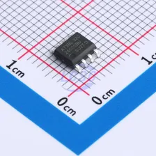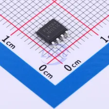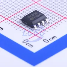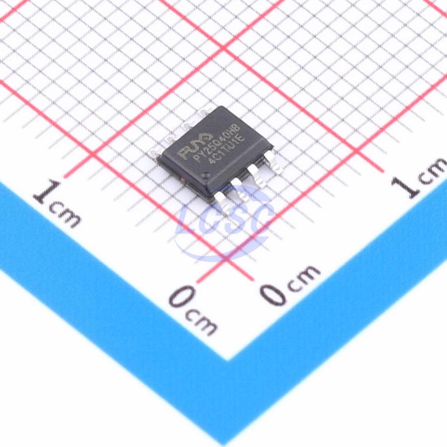
PY25Q40HB-SSH-IR
4Mbit 2.3V~3.6V 133MHz SPI SOP-8-150mil Memory
Every Order Guarantee
100% Authentic · 30-Day Return or Replacement · policy
3,270 in stock
#C50201613
Stock & price checked 6 days ago
| Quantity | Unit price | Pack price |
|---|---|---|
| 5+ | ₹33.80 | ₹169.00 |
| 50+ | ₹26.68 | ₹1,334.00 |
| 150+ | ₹23.64 | ₹3,546.00 |
| 500+ | ₹19.83 | ₹9,915.00 |
| 2,500+ | ₹18.14 | ₹45,350.00 |
| 4,000+ | ₹17.12 | ₹68,480.00 |
5 × ₹33.80
₹169.00
excl. GST
₹199.42 incl. 18% GST
- Dispatch in 7–10 working days
- GST invoice with every order
- Standard pack: 4,000 per reel
PY25Q40HB-SSH-IR
₹169.00 for 5 + GST
Specifications
- Operating Temperature
- -40℃~+85℃
- Features
- Write enable latch;Power-on reset;Hardware write protection;Software write protection;Absolute write protection
- Memory Size
- 4Mbit
- Voltage - Supply
- 2.3V~3.6V
- Program / Erase Cycles
- 100,000 cycles
- Clock Frequency
- 133MHz
- Data Retention - TDR (Year)
- 20 Years
- Block Erase Time(tBE)
- 150ms
- Page Programming Time (Tpp)
- 500us
- Standby Supply Current
- 15uA
- Interface
- SPI
Packaging & compliance
- RoHS
- RoHS
- Lifecycle
- Active
- Packaging
- Tape & Reel (TR)
- Standard pack
- 4,000 / Reel
- Sold per
- Piece
- Minimum order
- 5 (multiples of 5)
- Unit weight
- 0.06 g
Overview
The PY25Q40HB is a serial interface Flash memory device designed for high-volume consumer applications that require mapping program code from Flash memory into embedded or external RAM for execution. The device's flexible erase architecture and sector erase granularity also make it an ideal choice for data storage, eliminating the need for additional data storage devices. The device's erase block sizes are optimized to meet the demands of today's code and data storage applications. By optimizing erase block sizes, storage space can be utilized more efficiently. Since certain code modules and data storage segments must reside independently within their respective erase regions, the waste and unused storage space caused by large sector and block erases are significantly reduced compared to Flash devices that employ large sector and block erases. This improved storage space efficiency allows additional code routines and data storage segments to be added while maintaining the same overall device density. The device also includes an additional 3×512-byte security register with OTP (One-Time Programmable) locking, which can be used for purposes such as device serialization, system-level electronic serial number storage, and lock key storage. The device is designed for a wide variety of system designs, supporting read, program, and erase operations over a wide supply voltage range of 2.3V to 3.6V. No separate voltage is required for programming and erasing.
Same category