Nexperia
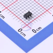
74LVC245APW,118Schmitt trigger 1.2V~3.6V 8 1 2.9ns@3.3V,50pF TSSOP-20 Buffers, Drivers, Receivers, Transceivers RoHS
From
₹28.44
2,50,360 in stock
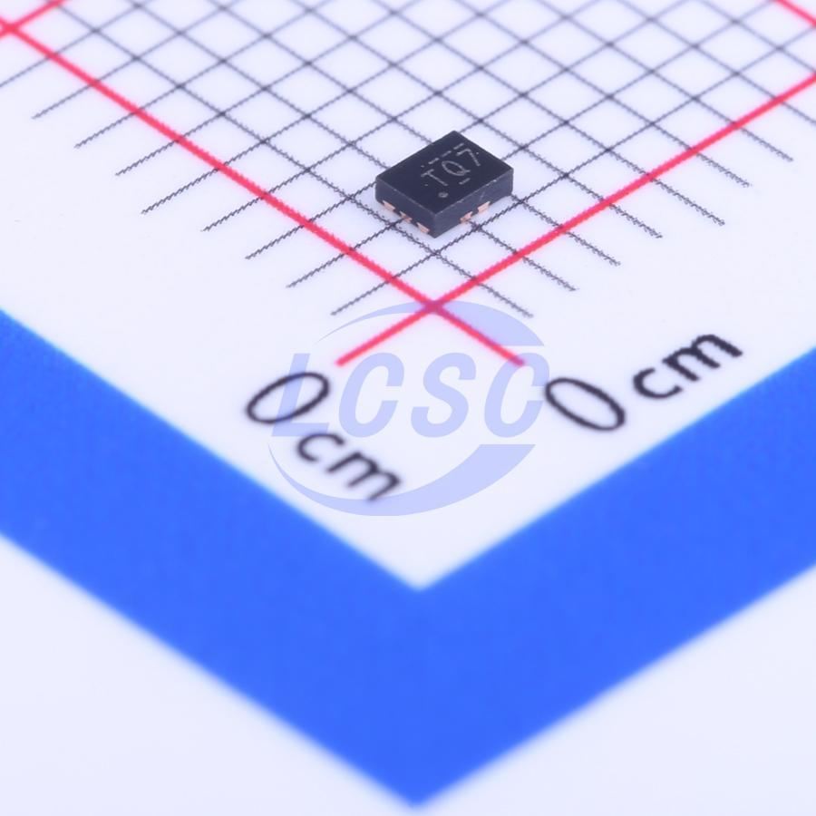
1.2V~3.6V 2 2 2.4ns@3.3V,30pF WQFN-10(1.4x1.8) Buffers, Drivers, Receivers, Transceivers RoHS
Dual-Bit Dual-Supply Bus Transceiver with Configurable Level-Shifting, Voltage Translation and Tri-State Outputs
Every Order Guarantee
100% Authentic · 30-Day Return or Replacement · policy
1,63,585 in stock
#C128418
Stock & price checked 6 days ago
| Quantity | Unit price | Pack price |
|---|---|---|
| 5+ | ₹47.35 | ₹236.75 |
| 50+ | ₹37.18 | ₹1,859.00 |
| 150+ | ₹32.81 | ₹4,921.50 |
| 500+ | ₹25.30 | ₹12,650.00 |
| 3,000+ | ₹22.87 | ₹68,610.00 |
| 6,000+ | ₹21.42 | ₹1,28,520.00 |
5 × ₹47.35
₹236.75
excl. GST
₹279.37 incl. 18% GST
SN74AVC2T245RSWR
₹236.75 for 5 + GST
This dual-bit noninverting bus transceiver uses two separate configurable power-supply rails. The A port is designed to track VCCA. VCCA accepts any supply voltage from 1.2 V to 3.6 V. The B port is designed to track VCCB. VCCB accepts any supply voltage from 1.2 V to 3.6 V. This allows for universal low-voltage bidirectional translation between any of the 1.2 V, 1.5 V, 1.8 V, 2.5 V, and 3.3 V voltage nodes. The SN74AVC2T245 is designed for asynchronous communication between two data buses. The logic levels of the direction-control (DIR) input and the output-enable (OE) activate either the B-port outputs or the A-port outputs or place both output ports into the high-impedance mode. The device transmits data from the A bus to the B bus when the B-port outputs are activated and from the B bus to the A bus when the A-port outputs are activated. The input circuitry on both A and B ports always is active and must have a logic HIGH or LOW level applied to prevent excess ICC and ICCZ. The SN74AVC2T245 control pins (DIR1, DIR2, and OE) are supplied by VCCA. This device is fully specified for partial-power-down applications using Ioff. The Ioff circuitry disables the outputs, preventing damaging current backflow through the device when it is powered down. The VCC isolation feature ensures that if either VCC input is at GND, both ports are in the high-impedance state. To ensure the high-impedance state during power up or power down, OE must be connected to VCC through a pull-up resistor; the minimum value of the resistor is determined by the current-sinking capability of the driver.
Same category
Nexperia
74LVC245APW,118Schmitt trigger 1.2V~3.6V 8 1 2.9ns@3.3V,50pF TSSOP-20 Buffers, Drivers, Receivers, Transceivers RoHS
From
₹28.44
2,50,360 in stock
TI
SN74LV1T125DBVR1.6V~5.5V 1 1 5.5ns@5V,15pF SOT-23-5 Buffers, Drivers, Receivers, Transceivers RoHS
From
₹21.35
2,07,155 in stock
TI
SN74LVC2G07DBVR1.65V~5.5V 1 2 3.7ns@3.3V,50pF SOT-23-6 Buffers, Drivers, Receivers, Transceivers RoHS
From
₹12.09
1,51,380 in stock
TI
SN74LVC1G17DCKRSchmitt trigger 1.65V~5.5V 1 1 4.6ns@3.3V,50pF SC-70-5 Buffers, Drivers, Receivers, Transceivers RoHS
From
₹9.49
1,13,030 in stock