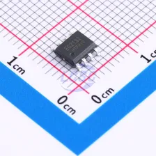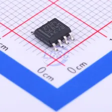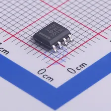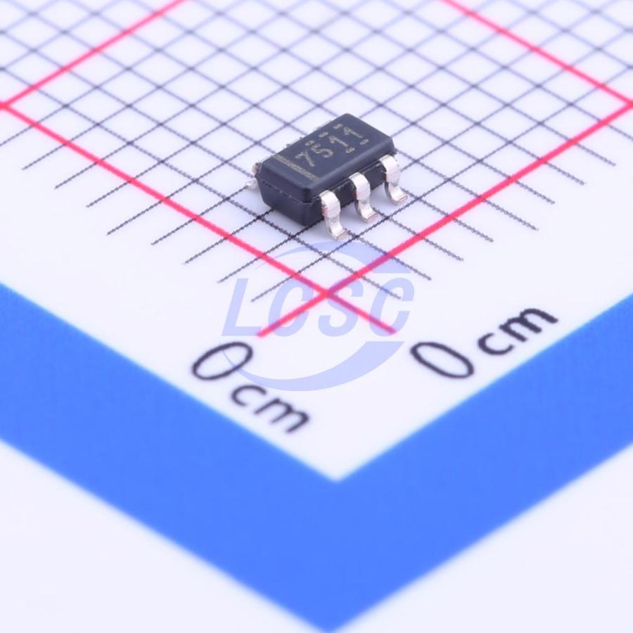
UCC27511DBVR
4.5V~18V 8A 4A SOT-23-6 Gate Drivers RoHS
Single-Channel, High-Speed, Low-Side Gate Driver (With Peak Source and Peak Sink)
- Manufacturer
- TI
- Manufacturer part #
- UCC27511DBVR
- Store part #
- C191027
- Package / case
- SOT-23-6
- Category
- Gate Drivers
- Packaging
- Tape & Reel (TR)
Every Order Guarantee
100% Authentic · 30-Day Return or Replacement · policy
6,891 in stock
#C191027
Stock & price checked 6 days ago
| Quantity | Unit price | Pack price |
|---|---|---|
| 1+ | ₹80.84 | ₹80.84 |
| 10+ | ₹64.97 | ₹649.70 |
| 30+ | ₹57.15 | ₹1,714.50 |
| 100+ | ₹49.11 | ₹4,911.00 |
| 500+ | ₹41.52 | ₹20,760.00 |
| 1,000+ | ₹39.12 | ₹39,120.00 |
1 × ₹80.84
₹80.84
excl. GST
₹95.39 incl. 18% GST
- Dispatch in 7–10 working days
- GST invoice with every order
- Standard pack: 3,000 per reel
UCC27511DBVR
₹80.84 for 1 + GST
Specifications
- Input Logic Level - Low
- 1V~1.2V
- Low Level Delay Time
- 13ns
- High Level Delay Time
- 13ns
- Quiescent Current
- 100uA
- Input Logic Level - High
- 2.2V~2.4V
- Voltage - Supply
- 4.5V~18V
- Operating Temperature
- -40℃~+140℃
- Driven Configuration
- Low Side
- Current - Output Low(IOL)
- 8A
- Rise Time
- 8ns
- Fall Time
- 7ns
- Features
- Enable shutdown;Interleaved conduction protection
- Current - Output High(IOH)
- 4A
- Load Type
- MOSFET;IGBT
Packaging & compliance
- RoHS
- ROHS3 Compliant
- Lifecycle
- Active
- ECCN
- EAR99
- Packaging
- Tape & Reel (TR)
- Standard pack
- 3,000 / Reel
- Sold per
- Piece
- Minimum order
- 1
- Unit weight
- 0.057 g
Overview
The UCC27511 and UCC27512 single-channel, highspeed, low-side gate-driver device can effectively drive MOSFET and IGBT power switches. Using a design that inherently minimizes shoot-through current, UCC27511 and UCC27512 are capable of sourcing and sinking high peak-current pulses into capacitive loads offering rail-to-rail drive capability and extremely small propagation delay, typically 13 ns. UCC27511 features a dual-input design which offers flexibility of implementing both inverting (IN– pin) and noninverting [IN+ pin) configuration with the same device. Either IN+ or IN– pin can be used to control the state of the driver output. The unused input pin can be used for enable and disable functions. For safety purpose, internal pullup and pulldown resistors on the input pins ensure that outputs are held low when input pins are in floating condition. Hence the unused input pin is not left floating and must be properly biased to ensure that driver output is in enabled for normal operation. The input pin threshold of the UCC27511 device is based on TTL and CMOS-compatible low-voltage logic which is fixed and independent of the VDD supply voltage. Wide hysteresis between the high and low thresholds offers excellent noise immunity. The UCC27511 and UCC27512 provides 4-A source, 8-A sink (asymmetrical drive) peak-drive current capability. Strong sink capability in asymmetrical drive boosts immunity against parasitic, Miller turnon effect. The UCC27511 device also features a unique split output configuration where the gate-drive current is sourced through OUTH pin and sunk through OUTL pin. This unique pin arrangement allows the user to apply independent turnon and turnoff resistors to the OUTH and OUTL pins respectively and easily control the switching slew rates. UCC27511 and UCC27512 are designed to operate over a wide VDD range of 4.5 to 18 V and wide temperature range of -40°C to 140°C
Applications
- Switched-Mode Power Supplies
- DC-to-DC Converters
- Companion Gate-Driver Devices for Digital Power Controllers
- Solar Power
- Motor Control
- UPS
- Gate Driver for Emerging Wide Band-Gap Power Devices (such as GaN)
Key features
- Low-Cost Gate-Driver Device Offering Superior Replacement of NPN and PNP Discrete Solutions
- 4-A Peak Source and 8-A Peak Sink
- Asymmetrical Drive
- Strong Sink Current Offers Enhanced Immunity Against Miller Turnon
- Split Output Configuration (Allows Easy and Independent Adjustment of Turnon and Turnoff Speeds) in the UCC27511 Saves 1 Diode
- Fast Propagation Delays (13-ns Typical)
- Fast Rise and Fall Times (9-ns and 7-ns Typical)
- 4.5-V to 18-V Single Supply Range
- Outputs Held Low During VDD UVLO (Ensures Glitch-Free Operation at Power Up and Power Down)
- TTL and CMOS Compatible Input-Logic Threshold (Independent of Supply Voltage)
- Hysteretic-Logic Thresholds for High-Noise Immunity
- Dual-Input Design (Choice of an Inverting (IN– Pin) or Noninverting [IN+ Pin) Driver Configuration)
- Unused Input Pin can be Used for Enable or Disable Function
- Output Held Low When Input Pins Are Floating
- Input Pin Absolute Maximum Voltage Levels Not Restricted by VDD Pin Bias Supply Voltage
- Operating Temperature Range of -40°C to 140°C
- 6-Pin DBV (SOT-23) and 6-Pin DRS (3-mm×3-mm WSON With Exposed Thermal Pad) Package Options
Alternatives
Similar parts — check the datasheet before substituting.
| Part | Manufacturer | Package | Stock | Price from (excl. GST) | Action | |
|---|---|---|---|---|---|---|
 | UCC27511DBVT#C154934TI · SOT-23-6 | TI | SOT-23-6 | 753 | ₹118.37 · 753 in stock | View |
 | UCC27511ADBVR#C2676982TI · SOT-23-6 | TI | SOT-23-6 | 11,375 | ₹51.07 · 11,375 in stock | View |
 | UCC27511ADBVT#C2676984TI · SOT-23-6 | TI | SOT-23-6 | On request | Price on request | Quote |
 | JSM27511#C19077362JSMSEMI · SOT-23-6 | JSMSEMI | SOT-23-6 | 445 | ₹46.60 · 445 in stock | View |
 | UCC27511DBVT-JSM#C7466359JSMSEMI · SOT-23-6 | JSMSEMI | SOT-23-6 | 3,646 | ₹88.14 · 3,646 in stock | View |
Same category