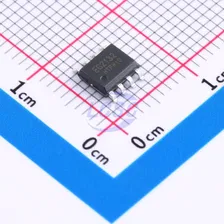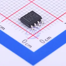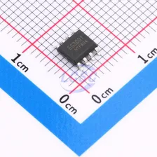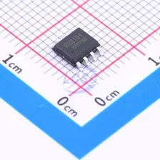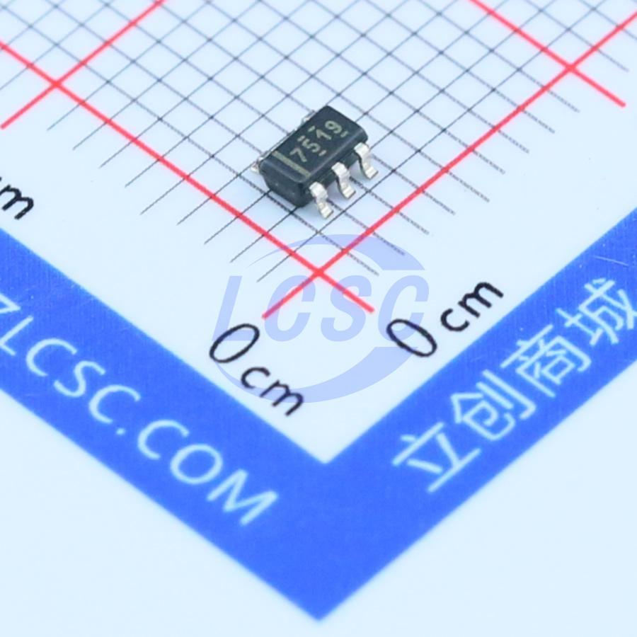
UCC27519DBVR
Low Side Gate Driver IC MOSFET IGBT SOT-23-5
Single-channel high-speed low-side gate driver (based on CMOS input threshold and with a peak pull/sink current drive capability of 4A)
- Manufacturer
- TI
- Manufacturer part #
- UCC27519DBVR
- Store part #
- C93674
- Package / case
- SOT-23-5
- Category
- Gate Drivers
- Packaging
- Tape & Reel (TR)
Every Order Guarantee
100% Authentic · 30-Day Return or Replacement · policy
5,731 in stock
#C93674
Stock & price checked 6 days ago
| Quantity | Unit price | Pack price |
|---|---|---|
| 1+ | ₹77.12 | ₹77.12 |
| 10+ | ₹62.78 | ₹627.80 |
| 30+ | ₹55.61 | ₹1,668.30 |
| 100+ | ₹48.66 | ₹4,866.00 |
| 500+ | ₹39.11 | ₹19,555.00 |
| 1,000+ | ₹36.92 | ₹36,920.00 |
1 × ₹77.12
₹77.12
excl. GST
₹91.00 incl. 18% GST
- Dispatch in 7–10 working days
- GST invoice with every order
- Standard pack: 3,000 per reel
UCC27519DBVR
₹77.12 for 1 + GST
Specifications
- Low Level Delay Time
- 17ns
- High Level Delay Time
- 17ns
- Voltage - Supply
- 4.5V~18V
- Operating Temperature
- -40℃~+140℃
- Driven Configuration
- Low Side
- Current - Output Low(IOL)
- 4A
- Rise Time
- 8ns
- Fall Time
- 7ns
- Features
- Enable shutdown
- Current - Output High(IOH)
- 4A
- Load Type
- MOSFET;IGBT
Packaging & compliance
- RoHS
- ROHS3 Compliant
- Lifecycle
- Active
- ECCN
- EAR99
- Packaging
- Tape & Reel (TR)
- Standard pack
- 3,000 / Reel
- Sold per
- Piece
- Minimum order
- 1
- Unit weight
- 0.033 g
Overview
The UCC27518 and UCC27519 single-channel high-speed low-side gate driver devices effectively drive MOSFET and IGBT power switches. The UCC27518 and UCC27519 employ a design that minimizes shoot-through current, delivering high peak source/sink current pulses to capacitive loads while providing rail-to-rail drive capability and ultra-short propagation delay (17ns typical). At VDD = 12V, the UCC27518 and UCC27519 provide peak sink/source (symmetrical drive) current capability of 4A. The UCC27518 and UCC27519 feature a wide VDD range of 4.5V to 18V and a wide temperature range of -40°C to 140°C. When the VDD operating range is exceeded, an internal UVLO circuit on the VDD pin holds the output low. These devices not only operate at low voltages below 5V but also offer best-in-class switching performance, making them ideal for driving emerging wide-bandgap power switch devices such as GaN power semiconductors. The input pin thresholds of the UCC27518 and UCC27519 are based on CMOS logic, where the threshold voltage is a function of the VDD supply voltage. The typical input high threshold (V1N-H) is 55% of VDD, while the typical input low threshold (V1N-L) is 39% of VDD. The wide hysteresis between the two thresholds (typically 16% of VDD) provides excellent noise immunity and allows users to introduce delay by placing an RC circuit between the input PWM signal and the INx pin of the device. The UCC27518 and UCC27519 also feature a floating-capable enable function on the EN pin. Leaving the EN pin unconnected enables pin compatibility between the UCC27518/UCC27519 and the TPS2828/TPS2829, respectively. The voltage threshold of the EN pin is fixed and does not vary with the VDD pin bias voltage. The typical enable high threshold (VEN-H) is 2.1V, and the typical enable low threshold (VEN-L) is 1.25V.
Applications
- Switched-mode power supplies
- DC-DC converters
- Companion gate driver devices for digital power controllers
- Solar, motor control, UPS
- Gate drivers for emerging wide-bandgap power devices (e.g., GaN)
Key features
- Low-cost gate driver, superior alternative to NPN and PNP discrete solutions
- Pin-compatible with TI's TPS2828 and TPS2829 devices
- Symmetric 4A peak source and 4A peak sink drive
- Fast propagation delay (17ns typical)
- Fast rise and fall times (8ns and 7ns typical)
- 4.5V to 18V single-supply range
- Output held low during VDD UVLO (ensures glitch-free operation during power-up and power-down)
- CMOS input logic threshold (function of supply voltage with hysteresis)
- Hysteretic logic threshold for high noise immunity
- EN pin for enable function (can be left unconnected)
- Output held low when input pin is floating
- Input pin absolute maximum voltage level independent of VDD pin bias supply voltage
- Operating temperature range: -40°C to 140°C
- 5-pin DBV package (SOT-23)
Alternatives
Similar parts — check the datasheet before substituting.
| Part | Manufacturer | Package | Stock | Price from (excl. GST) | Action | |
|---|---|---|---|---|---|---|
 | UCC27519DBVT#C2676969TI · SOT-23-5 | TI | SOT-23-5 | 52 | ₹240.73 · 52 in stock | View |
 | UCC27518DBVR#C2653827TI · SOT-23-5 | TI | SOT-23-5 | 13 | ₹118.00 · 13 in stock | View |
 | UCC27519AQDBVRQ1#C2870531TI · SOT-23-5 | TI | SOT-23-5 | 99 | ₹209.48 · 99 in stock | View |
 | UCC27517ADBVR#C2653784TI · SOT-23-5 | TI | SOT-23-5 | 26,553 | ₹66.27 · 26,553 in stock | View |
 | UCC27517DBVT#C2877770TI · SOT-23-5 | TI | SOT-23-5 | 472 | ₹58.17 · 472 in stock | View |
Same category