RENESAS
AT25FF041A-UUN-T
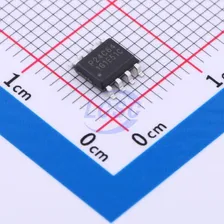
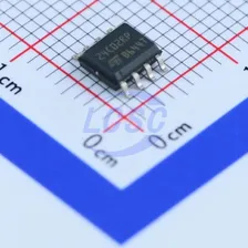
4Mbit 1.65V~3.6V 133MHz SPI WLCSP-8(1.7x1.8) Memory RoHS
WLCSP-8(1.7x1.8)ROHS3 CompliantActive
4-Mbit Flash Memory with Serial Peripheral Interface
Datasheet (PDF)
Every Order Guarantee
100% Authentic · 30-Day Return or Replacement · policy
1,000 in stock
#C7453693
Stock & price checked 5 days ago
| Quantity | Unit price | Pack price |
|---|---|---|
| 1+ | ₹218.98 | ₹218.98 |
| 10+ | ₹184.96 | ₹1,849.60 |
| 30+ | ₹163.69 | ₹4,910.70 |
| 100+ | ₹142.02 | ₹14,202.00 |
| 500+ | ₹132.05 | ₹66,025.00 |
| 1,000+ | ₹127.92 | ₹1,27,920.00 |
1 × ₹218.98
₹218.98
excl. GST
₹258.40 incl. 18% GST
- Dispatch in 7–10 working days
- GST invoice with every order
- Standard pack: 5,000 per reel
AT25FF041A-UUN-T
₹218.98 for 1 + GST
Specifications
- Operating Temperature
- -40℃~+85℃
- Memory Size
- 4Mbit
- Voltage - Supply
- 1.65V~3.6V
- Program / Erase Cycles
- 100,000 cycles
- Clock Frequency
- 133MHz
- Data Retention - TDR (Year)
- 20 Years
- Page Programming Time (Tpp)
- 7.8ms
- Standby Supply Current
- 30uA
- Interface
- SPI
Packaging & compliance
- RoHS
- ROHS3 Compliant
- Lifecycle
- Active
- ECCN
- EAR99
- Packaging
- Tape & Reel (TR)
- Standard pack
- 5,000 / Reel
- Sold per
- Piece
- Minimum order
- 1
- Unit weight
- 1 g
Overview
Key features
- Voltage Range: 1.65 V – 3.6 V
- 4-Mbit (2x2 Mbit physical block) Flash Memory
- Serial Peripheral Interface (SPI) compatible
- Supports SPI modes 0 and 3
- Supports dual output operation (1-1-2)
- Supports quad output operation (1-1-4)
- Supports quad I/O operation (1-4-4)
- Supports XiP operation (1-4-4, 0-4-4)
- 133 MHz maximum operating frequency
- Clock-to-output of 8 ns
- Flexible, optimized erase architecture for code + data storage applications
- Uniform 4-kByte block erase
- Uniform 32-kByte block erase
- Uniform 64-kByte block erase
- Full chip erase
- Flexible non-volatile block protection
- 1x128-byte factory-programmed unique identifier
- 3x128-byte, One Time Programmable (OTP) security registers
- Flexible programming
- Byte/Page program (1 to 256 Bytes)
- Sequential program mode capability
- Erase program suspend resume
- Software-controlled Reset and Terminate commands
- Hardware reset option (via HOLD pin)
- JEDEC hardware reset
- Non-volatile status register configuration option
- JEDEC standard manufacturer and device ID read methodology
- Serial Flash Discoverable Parameters (SFDP) version 1.6
- Low power dissipation
- 30 μA standby current (typical)
- 8.5 μA Deep Power-Down (DPD) current (typical)
- 7 nA Ultra-Deep Power-Down (UDPD) current (typical)
- 8.5 mA active read current (1-1-1-104 MHz)
- 8.5 mA program current
- 9.6 mA erase current
- User configurable and auto pin drive levels
- Endurance: 100,000 program/erase cycles
- Data Retention: 20 years
- Temperature Range: -40 ℃ to +85 ℃
- Industry standard green (Pb/Halide-free/RoHS Compliant) Package Options
- 8-lead SOIC (150-mil and 208-mil)
- 8-pad Ultra-thin DFN (2x3x0.6 mm)
- 8-ball WLCSP
- Die in Wafer Form (DWF)
Same category