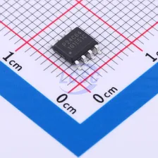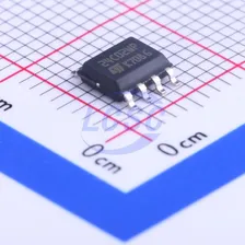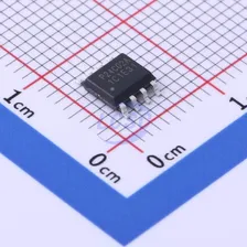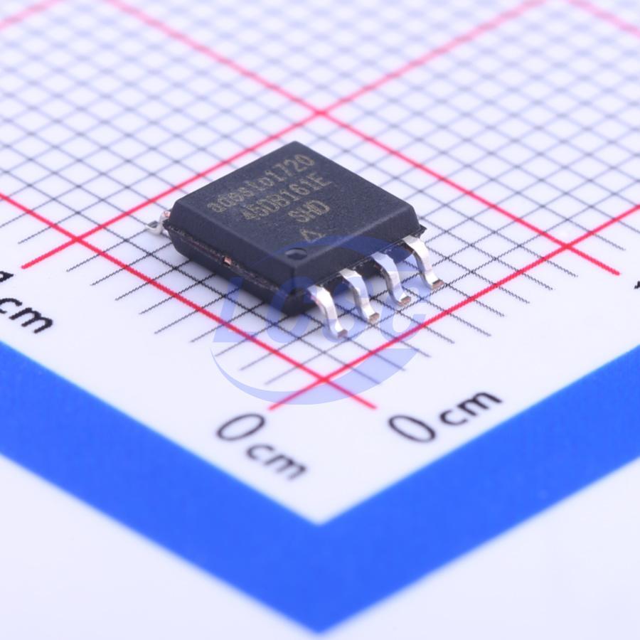
AT45DB161E-SHD-T
2.3V~3.6V 85MHz SPI SOIC-8-208mil Memory RoHS
SPI Serial Flash Memory
Every Order Guarantee
100% Authentic · 30-Day Return or Replacement · policy
6,781 in stock
#C64021
Stock & price checked 6 days ago
| Quantity | Unit price | Pack price |
|---|---|---|
| 1+ | ₹217.91 | ₹217.91 |
| 10+ | ₹185.38 | ₹1,853.80 |
| 30+ | ₹167.60 | ₹5,028.00 |
| 100+ | ₹147.44 | ₹14,744.00 |
| 500+ | ₹112.32 | ₹56,160.00 |
| 1,000+ | ₹108.19 | ₹1,08,190.00 |
1 × ₹217.91
₹217.91
excl. GST
₹257.13 incl. 18% GST
- Dispatch in 7–10 working days
- GST invoice with every order
- Standard pack: 2,000 per reel
AT45DB161E-SHD-T
₹217.91 for 1 + GST
Specifications
- Operating Temperature
- -40℃~+85℃
- Features
- Power-on reset;Hardware write protection;Software write protection;Absolute write protection
- Voltage - Supply
- 2.3V~3.6V
- Program / Erase Cycles
- 100,000 cycles
- Clock Frequency
- 85MHz
- Data Retention - TDR (Year)
- 20 Years
- Block Erase Time(tBE)
- 25ms@(4KB)
- Page Programming Time (Tpp)
- 4ms
- Standby Supply Current
- 25uA
- Interface
- SPI
Packaging & compliance
- RoHS
- ROHS Compliant
- Lifecycle
- Active
- ECCN
- EAR99
- Packaging
- Tape & Reel (TR)
- Standard pack
- 2,000 / Reel
- Sold per
- Piece
- Minimum order
- 1
- Unit weight
- 0.457 g
Overview
The Adesto AT45DB161E is a 2.3V or 2.5V minimum, serial-interface sequential access Flash memory ideally suited for a wide variety of digital voice, image, program code, and data storage applications. The AT45DB161E also supports the RapidS serial interface for applications requiring very high speed operation. Its 17,301,504 bits of memory are organized as 4,096 pages of 512 bytes or 528 bytes each. In addition to the main memory, the AT45DB161E also contains two SRAM buffers of 512/528 bytes each. The buffers allow receiving of data while a page in the main memory is being reprogrammed. Interleaving between both buffers can dramatically increase a system's ability to write a continuous data stream. In addition, the SRAM buffers can be used as additional system scratch pad memory, and E2PROM emulation (bit or byte alterability) can be easily handled with a self-contained three step read-modify-write operation. Unlike conventional Flash memories that are accessed randomly with multiple address lines and a parallel interface, the Adesto DataFlash uses a serial interface to sequentially access its data. The simple sequential access dramatically reduces active pin count, facilitates simplified hardware layout, increases system reliability, minimizes switching noise, and reduces package size. The device is optimized for use in many commercial and industrial applications where high-density, low-pin count, low-voltage, and low-power are essential. To allow for simple in-system re-programmability, the AT45DB161E does not require high input voltages for programming. The device operates from a single 2.3V to 3.6V or 2.5V to 3.6V power supply for the erase and program and read operations. The AT45DB161E is enabled through the Chip Select pin (CS) and accessed via a 3-wire interface consisting of the Serial Input (SI), Serial Output (SO), and the Serial Clock (SCK). All programming and erase cycles are self-timed.
Key features
- Single 2.3V - 3.6V or 2.5V - 3.6V supply
- Serial Peripheral Interface (SPI) compatible
- Supports SPI modes 0 and 3
- Supports RapidS™ operation
- Continuous read capability through entire array
- Up to 85MHz
- Low-power read option up to 15MHz
- Clock-to-output time (t_v) of 6ns maximum
- User configurable page size
- 512 bytes per page
- 528 bytes per page (default)
- Page size can be factory pre-configured for 512 bytes
- Two fully independent SRAM data buffers (512/528 bytes)
- Allows receiving data while reprogramming the main memory array
- Flexible programming options
- Byte/Page Program (1 to 512/528 bytes) directly into main memory
- Buffer Write
- Buffer to Main Memory Page Program
- Flexible erase options
- Page Erase (512/528 bytes)
- Block Erase (4KB)
- Sector Erase (128KB)
- Chip Erase (16-Mbits)
- Program and Erase Suspend/Resume
- Advanced hardware and software data protection features
- Individual sector protection
- Individual sector lockdown to make any sector permanently read-only
- 128-byte, One-Time Programmable (OTP) Security Register
- 64 bytes factory programmed with a unique identifier
- 64 bytes user programmable
- Hardware and software controlled reset options
- JEDEC Standard Manufacturer and Device ID Read
- Low-power dissipation
- 400nA Ultra-Deep Power-Down current (typical)
- 3μA Deep Power-Down current (typical)
- 25μA Standby current (typical at 20MHz)
- 11mA Active Read current (typical)
- Endurance: 100,000 program/erase cycles per page minimum
- Data retention: 20 years
- Complies with full industrial temperature range
- Green (Pb/Halide-free/RoHS compliant) packaging options
- 8-lead SOIC (0.150" wide and 0.208" wide)
- 8-pad Ultra-thin DFN (5x6x0.6mm)
- 9-ball Ultra-thin UBGA (6x6x0.6mm)
- Die in Wafer Form
Same category