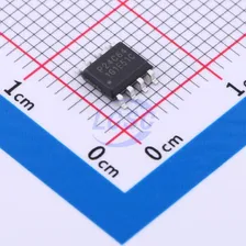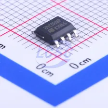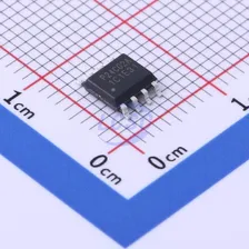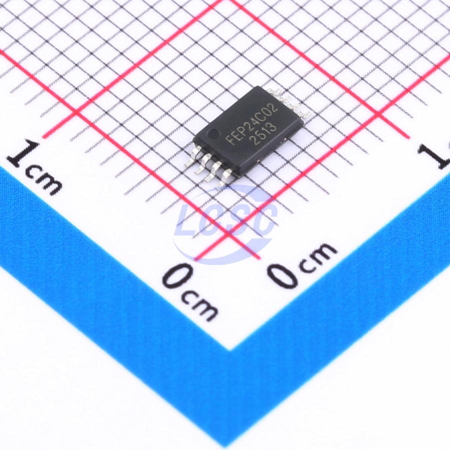
FEP24C02YTSSOP8G/TR
2Kbit 1MHz I2C TSSOP-8 Memory RoHS
Electrically Erasable Programmable Read Only Memory (EEPROM) Device
Every Order Guarantee
100% Authentic · 30-Day Return or Replacement · policy
1,590 in stock
#C48994850
Stock & price checked 5 days ago
| Quantity | Unit price | Pack price |
|---|---|---|
| 10+ | ₹10.08 | ₹100.80 |
| 100+ | ₹8.03 | ₹803.00 |
| 300+ | ₹7.00 | ₹2,100.00 |
| 3,000+ | ₹5.97 | ₹17,910.00 |
| 6,000+ | ₹5.36 | ₹32,160.00 |
| 9,000+ | ₹5.04 | ₹45,360.00 |
10 × ₹10.08
₹100.80
excl. GST
₹118.94 incl. 18% GST
- Dispatch in 7–10 working days
- GST invoice with every order
- Standard pack: 3,000 per reel
FEP24C02YTSSOP8G/TR
₹100.80 for 10 + GST
Specifications
- Operating Temperature
- -40℃~+85℃
- Features
- Hardware write protection function;Built-in power-on reset (POR);Noise suppression function
- Memory Size
- 2Kbit
- Voltage - Supply
- 1.65V~5.5V;0.8mA
- Clock Frequency
- 1MHz
- Access Time
- 900ns
- Data Retention - TDR (Year)
- 100 Years
- Write Cycle Time(tWC)
- 5ms
- Standby Supply Current
- 2uA
- Write Cycle Endurance
- 1,000,000 cycles
- Interface
- I2C
Packaging & compliance
- RoHS
- ROHS Compliant
- Lifecycle
- Active
- Packaging
- Tape & Reel (TR)
- Standard pack
- 3,000 / Reel
- Sold per
- Piece
- Minimum order
- 10 (multiples of 10)
- Unit weight
- 0.158 g
Overview
FEP24C02 is an industry-standard EEPROM device that communicates via an industry-standard two-wire interface. The device contains a 2K-bit (256×8) memory array organized in 8-byte pages. The EEPROM operates over a wide supply voltage range of 1.65V ~ 5.5V, suitable for most applications. The product offers low-power operation and low standby current. The device is available in lead-free, RoHS-compliant, halogen-free, and green packages. Available package types include 8-pin SOIC, TSSOP, UDFN, MSOP, and SOT23. The FEP24C02 is compatible with the standard I²C bus protocol. This simple bus consists of a serial clock (SCL) and serial data (SDA) signal. Using this bus protocol, a master device (such as a microcontroller) can typically control one or more slave devices, such as this FEP24C02. The bitstream transmitted over the SDA line contains a series of bytes used to identify a specific slave device, instructions, the address within that slave device, and a series of data (if applicable). The FEP24C02 also provides write protection via the WP pin to prevent overwriting data stored in the memory array. To prevent the state machine from entering an erroneous state during power-up sequences or power switching, an internal power-on reset circuit is integrated. During power-up, the device will not respond to any commands until the supply voltage VCC reaches an acceptable stable level above the reset threshold voltage. Once VCC exceeds the power-on reset threshold, the device is reset and enters standby mode. This also prevents any unintended write operations during the power-up phase. During power-down, once VCC falls below the power-on reset threshold voltage, the device enters standby mode. In addition, after receiving a stop command, the device will also be in standby mode as long as no internal write operation is in progress. However, sending commands is not valid unless VCC is within its operating voltage range.
Key features
- Two-wire serial interface, I²C compatible — bidirectional data transfer protocol
- Wide operating voltage range
- VCC = 1.65V ~ 5.5V
- Speed: 1 MHz (1.65V ~ 5.5V)
- Standby current (max): 1 μA at 5.5V
- Read current (max): 0.5 mA at 5.5V
- Write current (max): 0.8 mA at 5.5V
- Hardware data protection
- Write protect pin
- Sequential and random read modes
- Memory organization: 2 Kb (256 × 8)
- Page size: 8 bytes
- Page write mode
- Partial page write supported
- Self-timed write cycle: 5 ms (max)
- Input noise filtering, Schmitt trigger inputs
- High reliability
- Endurance: 1,000,000 erase/write cycles
- Data retention: 100 years
- Industrial grade
- Packages: SOIC, TSSOP, UDFN, SOT23, MSOP
- Lead-free, RoHS compliant, halogen-free, green
Same category