Every Order Guarantee
100% Authentic · 30-Day Return or Replacement · policy
1,141 in stock
#C2960662
Stock & price checked 5 days ago
| Quantity | Unit price | Pack price |
|---|---|---|
| 1+ | ₹9,724.40 | ₹9,724.40 |
| 30+ | ₹9,203.91 | ₹2,76,117.30 |
1 × ₹9,724.40
₹9,724.40
excl. GST
₹11,474.79 incl. 18% GST
- Dispatch in 7–10 working days
- GST invoice with every order
- Standard pack: 160 per tray
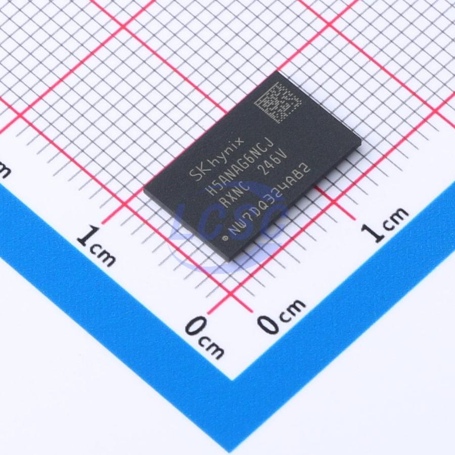
H5ANAG6NCJR-XNC
₹9,724.40 for 1 + GST
Specifications
- Features
- Auto self-refresh;Auto precharge function;Asynchronous reset function;Data mask function;Dynamic on-chip termination;ZQ calibration function;CRC function;Write leveling function
- Voltage - Supply
- -;-
Packaging & compliance
- RoHS
- ROHS Compliant
- Lifecycle
- Active
- Packaging
- Tray
- Standard pack
- 160 / Tray
- Sold per
- Piece
- Minimum order
- 1
- Unit weight
- 8.56 g
Overview
The H5ANAG4NCJR-xxC, H5ANAG8NCJR-xxC, H5ANAG6NCJR-xxC are a 16Gb CMOS Double Data Rate IV (DDR4) Synchronous DRAM, ideally suited for the main memory applications which requires large memory density and high bandwidth. 16Gb DDR4 SDRAMs offer fully synchronous operations referenced to both rising and falling edges of the clock. While all addresses and control inputs are latched on the rising edges of the CK (falling edges of the CK), Data, Data strobes and Write data masks inputs are sampled on both rising and falling edges of it. The data paths are internally pipelined and 8-bit prefetched to achieve very high bandwidth.
Key features
- VDD = VDDQ = 1.2V ± 0.06V
- Fully differential clock inputs (CK, CK) operation
- Differential Data Strobe (DQS, DQS)
- On chip DLL align DQ, DQS and DQS transition with CK transition
- DM masks write data-in at the both rising and falling edges of the data strobe
- All addresses and control inputs except data, data strobes and data masks latched on the rising edges of the clock
- Programmable CAS latency 9, 10, 11, 12, 13, 14, 15, 16, 17, 18, 19 and 20 supported
- Programmable additive latency 0, CL - 1, and CL - 2 supported (x4 / x8 only)
- Programmable CAS Write latency (CWL) = 9, 10, 11, 12, 14, 16, 18
- Programmable burst length 4 / 8 with both nibble sequential and interleave mode
- BL switch on the fly
- 16 banks
- Average Refresh Cycle (T case of 0°C ~ 95°C) - 7.8 us at 0°C ~ 85°C - 3.9 us at 85°C ~ 95°C
- JEDEC standard 78 ball FBGA (x4 / x8)
- Driver strength selected by MRS
- Dynamic On Die Termination supported
- Two Termination States such as RTT_PARK and RTT_NOM switchable by ODT pin
- Asynchronous RESET pin supported
- ZQ calibration supported
- TDQS (Termination Data Strobe) supported (x8 only)
- Write Levelization supported
- 8 bit pre-fetch
- This product in compliance with the RoHS directive.
- Internal Vref DQ level generation is available
- Write CRC is supported at all speed grades
- Maximum Power Saving Mode is supported
- TCAR (Temperature Controlled Auto Refresh) mode is supported
- LP ASR (Low Power Auto Self Refresh) mode is supported
- Fine Granularity Refresh is supported
- Per DRAM Addressability is supported
- Geardown Mode (1/2 rate, 1/4 rate) is supported
- Programmable Preamble for read and write is supported
- Self Refresh Abort is supported
- CA parity (Command/Address Parity) mode is supported
- Bank Grouping is applied, and CAS to CAS latency (tCCD_L, tCCD_S) for the banks in the same or different bank group accesses are available
- DBI (Data Bus Inversion) is supported (x8)
Same category