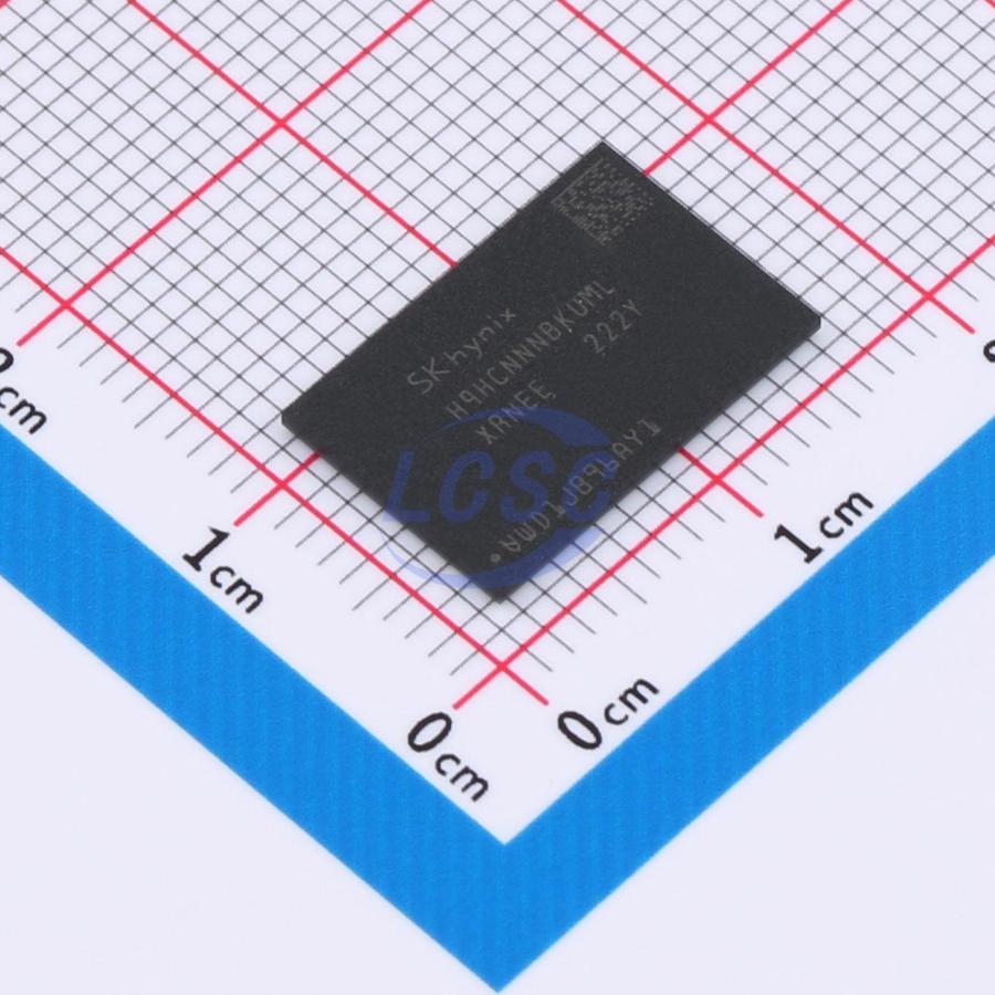
H9HCNNNBKUMLXR-NEE
16Gbit 4.266GHz LPDDR4 SDRAM FBGA-200(10x15) Memory RoHS
LPDDR4 16Gb
Every Order Guarantee
100% Authentic · 30-Day Return or Replacement · policy
1,400 in stock
#C21912322
Stock & price checked 5 days ago
| Quantity | Unit price | Pack price |
|---|---|---|
| 1+ | ₹8,709.63 | ₹8,709.63 |
| 30+ | ₹8,243.43 | ₹2,47,302.90 |
1 × ₹8,709.63
₹8,709.63
excl. GST
₹10,277.36 incl. 18% GST
- Dispatch in 7–10 working days
- GST invoice with every order
- Standard pack: 120 per tray
H9HCNNNBKUMLXR-NEE
₹8,709.63 for 1 + GST
Specifications
- Operating Temperature
- -25℃~+85℃
- Features
- Auto self-refresh;Auto precharge function;Asynchronous reset function;Write leveling function;ZQ calibration function
- Refresh Current
- 330uA
- Memory Size
- 16Gbit
- Voltage - Supply
- 7mA;1.06V~1.17V;1.7V~1.95V
- Clock Frequency
- 4.266GHz
- Memory Format
- LPDDR4 SDRAM
Packaging & compliance
- RoHS
- ROHS Compliant
- Lifecycle
- Active
- ECCN
- EAR99
- Packaging
- Tray
- Standard pack
- 120 / Tray
- Sold per
- Piece
- Minimum order
- 1
- Unit weight
- 0.25 g
Overview
LPDDR4-SDRAM is a high-speed synchronous DRAM device internally configured with either 1 or 2 channels. Single-channel is comprised of 8-banks with from 1 Gb to 16 Gb per channel density. Dual-channel is comprised of 8-banks with from 2 Gb to 32 Gb per channel density. LPDDR4 devices use multi cycle of single data rate architecture on the Command/Address (CA) bus to reduce the number of input pins in the system. The 6-bit CA bus contains command, address and bank information. Each command uses two clock cycles, during which command information is transferred on positive edge of the corresponding clock. These devices also use a double data rate architecture on the DQ pins to achieve high speed operation. The double data rate architecture is essentially an 16n prefetch architecture with an interface designed to transfer two data bits per DQ every clock cycle at the I/0 pins. Read and write accesses to the LPDDR4 SDRAMs are burst oriented; accesses start at a selected location and continue for a programmed number of locations in a programmed sequence. Prior to normal operation, the LPDDR4 SDRAM must be initialized.
Key features
- VDD1 = 1.8V (1.7V to 1.95V)
- VDD2 = 1.1V (1.06V to 1.17V)
- VDD2, VDDCA and VDDQ = 1.1V (1.06 to 1.17)
- VSSQ terminated DQ signals (DQ, DQS_t, DQS_c, DMI)
- Single data rate architecture for command and address; all control and address latched at rising edge of the clock
- Double data rate architecture for data Bus; two data accesses per clock cycle
- Differential clock inputs (CK_t, CK_c)
- Bi-directional differential data strobe (DQS_t, DQS_c)
- Source synchronous data transaction aligned to bi-directional differential data strobe (DQS_t, DQS_c)
- DMI pin support for write data masking and DBIdc functionality
- Programmable RL (Read Latency) and WL (Write Latency)
- Burst length: 16 (default), 32 and On-the-fly; On the fly mode is enabled by MRS
- Auto refresh and self refresh supported
- All bank auto refresh and directed per bank auto refresh supported
- Auto TCSR (Temperature Compensated Self Refresh)
- PASR (Partial Array Self Refresh) by Bank Mask and Segment Mask
- Background ZQ Calibration
Same category