Every Order Guarantee
100% Authentic · 30-Day Return or Replacement · policy
1,208 in stock
#C2802976
Stock & price checked 5 days ago
| Quantity | Unit price | Pack price |
|---|---|---|
| 1+ | ₹826.02 | ₹826.02 |
| 10+ | ₹716.91 | ₹7,169.10 |
| 30+ | ₹652.05 | ₹19,561.50 |
| 100+ | ₹586.33 | ₹58,633.00 |
| 500+ | ₹555.96 | ₹2,77,980.00 |
| 1,000+ | ₹542.30 | ₹5,42,300.00 |
1 × ₹826.02
₹826.02
excl. GST
₹974.70 incl. 18% GST
- Dispatch in 7–10 working days
- GST invoice with every order
- Standard pack: 2,000 per reel
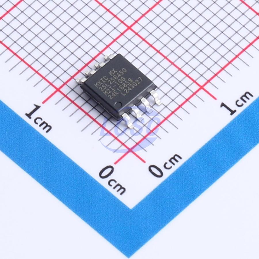
MX25L25645GM2I-10GTR
₹826.02 for 1 + GST
Specifications
- Operating Temperature
- -40℃~+85℃
- Features
- Write enable latch;Hardware write protection;Software write protection;Absolute write protection
- Memory Size
- 256Mbit
- Voltage - Supply
- 2.7V~3.6V
- Program / Erase Cycles
- 100,000 cycles
- Clock Frequency
- 133MHz
- Data Retention - TDR (Year)
- 20 Years
- Write Cycle Time(tWC)
- 40ms
- Interface
- SPI
Packaging & compliance
- RoHS
- RoHS
- Lifecycle
- Active
- ECCN
- 3A991b1a
- Packaging
- Tape & Reel (TR)
- Standard pack
- 2,000 / Reel
- Sold per
- Piece
- Minimum order
- 1
- Unit weight
- 0.24 g
Overview
MX25L25645G is a 3V, 256-megabit (organized as x1/x2/x4) CMOS MXSMIO® (Serial Multi I/O) flash memory. It supports SPI modes 0 and 3, operates from a single supply voltage ranging from 2.7V to 3.6V for read, erase, and program operations. The device is organized as 268,435,456 x 1-bit, 134,217,728 x 2-bit (Dual I/O mode), or 67,108,864 x 4-bit (Quad I/O mode). It supports Single I/O, Dual I/O, and Quad I/O protocols, including DTR (Double Transfer Rate) mode, with a maximum clock frequency of 133MHz across all protocols. The device features latch-up protection with a current tolerance of 100 mA over a voltage range of -1V to Vcc+1V, and a low Vcc write inhibit voltage of 1.5V to 2.5V. It supports fast read instructions (FAST_READ, 2READ, DREAD, 4READ, QREAD), configurable dummy cycles for fast read operations, and performance-enhanced modes — XIP (Execute In Place) and QPI mode. Memory is organized into uniform 4KB sectors, or uniform blocks of 32KB or 64KB, with any block individually erasable. Programming features include a 256-byte page buffer and Quad Input/Output Page Program (4PP) for enhanced programming performance. Typical endurance is 100,000 erase/program cycles with a 20-year data retention. Software features include: 1-byte command code; advanced security features such as block protect with BP0–BP3 and T/B status bits defining protected area size; individual sector protection (solid protection); an additional 4K-bit security OTP memory with identifier, factory-lockable or customer-lockable; software reset; program/erase suspend and resume; electronic ID supporting JEDEC-standard 1-byte manufacturer ID and 2-byte device ID, RES command for reading 1-byte device ID, and REMS command for reading 1-byte manufacturer ID and 1-byte device ID; Serial Flash Discoverable Parameters (SFDP) mode support. Hardware features include: serial clock input, and serial data input or serial data I/O pins for 2x I/O and 4x I/O read modes.
Key features
- SPI support — Mode 0 and Mode 3
- Single supply operation: 2.7V to 3.6V for read, erase, and program operations
- Memory organization: 268,435,456 x 1-bit, or 134,217,728 x 2-bit (Dual I/O mode), or 67,108,864 x 4-bit (Quad I/O mode)
- Protocol support: Single I/O, Dual I/O, and Quad I/O
- Latch-up protection: withstands 100 mA current in the range of -1V to Vcc+1V
- Low Vcc write inhibit voltage: 1.5V to 2.5V
- Fast read: up to 133MHz clock frequency for all protocols; supports FAST_READ, 2READ, DREAD, 4READ, QREAD instructions; DTR mode support; configurable dummy cycles for fast read operations
- Performance-enhanced mode support — XIP (Execute In Place)
- Quad peripheral interface provided
- Memory organization: uniform 4KB sectors, or uniform 32KB/64KB blocks; individually erasable blocks
- Programming: 256-byte page buffer; quad I/O page programming for enhanced programming performance
- Typical erase/program cycles: 100,000
- Data retention: 20 years
- Software features: 1-byte command code; advanced security (block lock protection, individual sector protection); additional 4K-bit security OTP memory (with identifier, factory/customer lockable); software reset; program/erase suspend and resume; electronic identification (JEDEC manufacturer ID and device ID, RES command, REMS command); Serial Flash Discoverable Parameters (SFDP) mode support
- Hardware features: serial clock input pin; serial data I/O pins (supports 2x I/O and 4x I/O read modes)
Same category