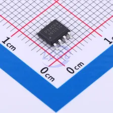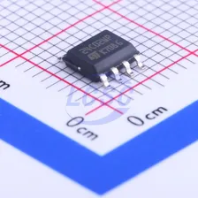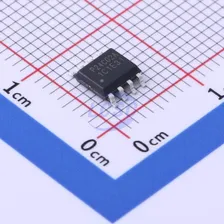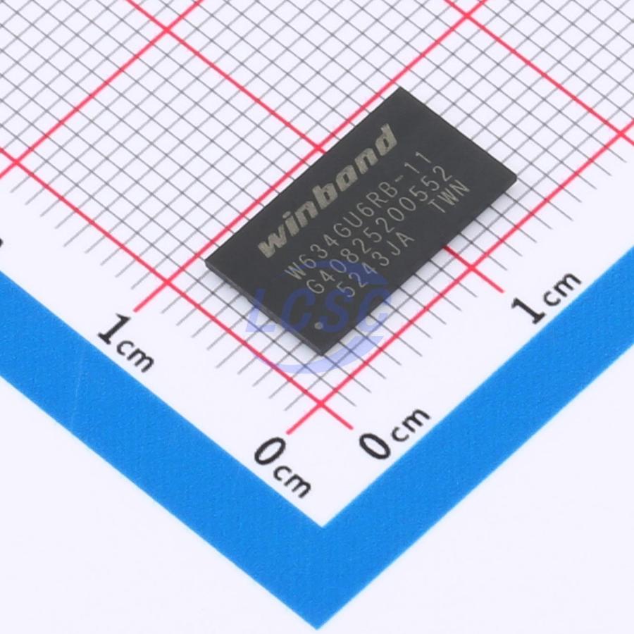
W634GU6RB-11
4Gbit 933MHz DDR3L SDRAM VFBGA-96(13x7.5) Memory RoHS
Every Order Guarantee
100% Authentic · 30-Day Return or Replacement · policy
2,850 in stock
#C29801372
Stock & price checked 5 days ago
| Quantity | Unit price | Pack price |
|---|---|---|
| 1+ | ₹2,187.75 | ₹2,187.75 |
| 10+ | ₹2,107.57 | ₹21,075.70 |
| 30+ | ₹1,968.49 | ₹59,054.70 |
| 100+ | ₹1,847.03 | ₹1,84,703.00 |
1 × ₹2,187.75
₹2,187.75
excl. GST
₹2,581.55 incl. 18% GST
- Dispatch in 7–10 working days
- GST invoice with every order
- Standard pack: 198 per tray
W634GU6RB-11
₹2,187.75 for 1 + GST
Specifications
- Operating Temperature
- -40℃~+95℃
- Features
- Auto self-refresh;Auto precharge function;Data mask function;Write leveling function;ZQ calibration function;Asynchronous reset function;Dynamic on-chip termination
- Memory Size
- 4Gbit
- Voltage - Supply
- 1.283V~1.45V;-
- Clock Frequency
- 933MHz
- Memory Format
- DDR3L SDRAM
Packaging & compliance
- RoHS
- ROHS Compliant
- Lifecycle
- Active
- ECCN
- EAR99
- Packaging
- Tray
- Standard pack
- 198 / Tray
- Sold per
- Piece
- Minimum order
- 1
- Unit weight
- 1.706 g
Overview
Winbond W631GU6NB-11 is a 1.5V, 512Mbit low-power double data rate 3L synchronous dynamic random access memory (DDR3L SDRAM) device. The device is internally configured as 8 banks with 16-bit I/O, organized as 32M × 8 banks × 16 bits. It employs a double data rate architecture for high-speed operation. This double data rate architecture is essentially an 8n-prefetch architecture, with an interface designed to transfer two data words per clock cycle at the I/O pins. For DDR3L SDRAM, a single read or write access consists of an 8n-bit wide, one-clock-cycle data transfer at the internal DRAM core, and eight corresponding n-bit wide, half-clock-cycle data transfers at the I/O pins. The device is designed to comply with key DDR3L DRAM features such as posted CAS# with additive latency, write latency equal to read latency minus 1, on-die termination (ODT), and dynamic ODT for write operations. All control and address inputs are synchronous to a pair of externally supplied differential clocks. Inputs are latched at the crossing point of the differential clock (rising edge of CK and falling edge of CK#). All I/O are synchronous to a pair of bidirectional differential data strobes (DQS, DQS#), which are edge-aligned with data during reads and center-aligned with data during writes. The device supports the following features: programmable CAS latency, programmable additive latency, programmable burst length (BL8, BC4, and BC4 via mode register set (MRS)), and programmable partial array self-refresh (PASR).
Key features
- Supply voltage VDD = VDDQ = 1.5V ±0.075V
- 8n-bit prefetch architecture
- Differential clock inputs (CK, CK#)
- Differential data strobe (DQS, DQS#)
- Data strobe (DQS, DQS#) edge-aligned with data during reads, center-aligned during writes
- Data Mask (DM) masks data during writes
- All address and control inputs latched at the crossing of CK and CK#
- Programmable CAS Latency: 5, 6, 7, 8, 9, 10, 11, 12, 13, 14
- Programmable Additive Latency: 0, CL-1, CL-2
- Programmable Burst Length: 8, 4 (via BC4 or BL8 mode)
- Programmable Partial Array Self-Refresh (PASR)
- Auto Self-Refresh (ASR) and Self-Refresh Temperature (SRT)
- Dynamic ODT (Rtt_WR) support
- Programmable output driver impedance (RZQ/7, RZQ/6, RZQ/5)
- Programmable ODT impedance (RZQ/6, RZQ/7, RZQ/4, RZQ/2, disabled)
- Programmable Write Recovery (WR)
- Programmable CWL: 5, 6, 7, 8, 9, 10, 11, 12, 13, 14
- Programmable DLL reset
- Programmable DLL enable/disable
- Programmable output disable
- Programmable Multi-Purpose Register (MPR)
- Programmable test mode
- Programmable precharge powerdown DLL
- Programmable write leveling
- Programmable ZQ calibration
- Programmable reset
- Programmable initialization
- Programmable mode register
- Programmable command truth table
- Programmable CKE truth table
- Programmable simplified state diagram
- Programmable electrical characteristics
- Programmable maximum ratings
- Programmable operating temperature conditions
- Programmable DC and AC operating conditions
- Programmable recommended DC operating conditions
- Programmable input and output leakage current
- Programmable interface test conditions
- Programmable DC and AC input measurement levels
- Programmable DC and AC input levels (single-ended command and address signals)
- Programmable DC and AC input levels (single-ended data signals)
- Programmable differential swing requirements (clock (CK - CK#) and strobe (DQS - DQS#))
- Programmable single-ended requirements for differential signals
- Programmable differential input crosspoint voltage
- Programmable slew rate definition for single-ended input signals
- Programmable slew rate definition for differential input signals
- Programmable DC and AC output measurement levels
- Programmable output slew rate definitions and requirements
- Programmable single-ended output slew rate
- Programmable differential output slew rate
- Programmable output driver DC electrical characteristics
- Programmable output driver temperature and voltage sensitivity
- Programmable ODT levels and characteristics
- Programmable ODT levels and I-V characteristics
- Programmable ODT DC electrical characteristics
- Programmable ODT temperature and voltage sensitivity
- Programmable RTTPU and RTTPD design guidelines
- Programmable ODT timing definitions
Same category