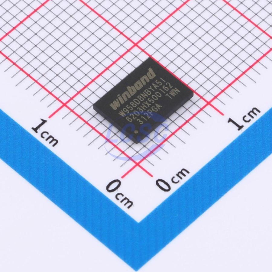
W958D8NBYA5I
256Mbit 1.7V~2V 200MHz TFBGA-24(6x8) Memory RoHS
256Mb HyperRAM
Every Order Guarantee
100% Authentic · 30-Day Return or Replacement · policy
1,130 in stock
#C7420405
Stock & price checked 5 days ago
| Quantity | Unit price | Pack price |
|---|---|---|
| 1+ | ₹2,397.75 | ₹2,397.75 |
| 10+ | ₹2,318.19 | ₹23,181.90 |
| 30+ | ₹2,180.08 | ₹65,402.40 |
| 100+ | ₹2,059.74 | ₹2,05,974.00 |
1 × ₹2,397.75
₹2,397.75
excl. GST
₹2,829.35 incl. 18% GST
- Dispatch in 7–10 working days
- GST invoice with every order
- Standard pack: 480 per tray
W958D8NBYA5I
₹2,397.75 for 1 + GST
Specifications
- Operating Temperature
- -40℃~+85℃
- Memory Size
- 256Mbit
- Voltage - Supply
- 1.7V~2V
- Clock Frequency
- 200MHz
- Standby Supply Current
- 1.2mA
Packaging & compliance
- RoHS
- ROHS Compliant
- Lifecycle
- Active
- ECCN
- EAR99
- Packaging
- Tray
- Standard pack
- 480 / Tray
- Sold per
- Piece
- Minimum order
- 1
- Unit weight
- 0.08 g
Overview
HyperBus is a low pin count DDR interface that enables high-speed read and write throughput. The DDR protocol transfers two data bytes per clock cycle on the DQ I/O signals. Read and write transactions on HyperBus consist of a series of 16-bit wide, one-clock-cycle data transfers on the internal HyperRAM array, along with two corresponding 8-bit wide, half-clock-cycle data transfers on the DQ signals. All inputs and outputs are LV-CMOS compatible. Command, address, and data information are transferred through eight HyperBus DQ[7:0] signals. The clock (CK#, CK) is used by HyperBus slave devices to capture information when receiving commands, addresses, or data on the DQ signals. Command or address values are center-aligned with clock transitions. Each transaction begins with the assertion of CS# and the command-address (CA) signals, followed by clock transitions to transfer six CA bytes, then an initial access latency and read/write data transfer, until CS# is deasserted. Read and write transactions require two clock cycles to define the target row address and burst type, followed by an initial access latency of tACC. During the CA portion of the transaction, the memory indicates whether an additional delay for the required refresh time (tRFH) has been added to the initial latency by driving the RWDS signal high. During CA, the third clock cycle specifies the target word address within the target row. In read and write transactions, after the initial data value is output (or input), additional data can be read from (or written to) the row in subsequent clock cycles in either wrap or linear order. When configured for linear burst mode, the device automatically fetches the next consecutive row from the memory array to support continuous linear bursts. Accessing the next row in the array concurrently with ongoing read/write data transfers enables linear sequential burst operation, delivering a sustained data rate of 500 MB/s (1 byte (8-bit data bus) × 2 (data clock edges) × 250 MHz = 500 MB/s).
Key features
- Interface: HyperBus
- Power supply: 1.7V~2.0V
- Maximum clock rate: 250MHz
- Double-Data Rate (DDR) Up to 500 MB/s
- Clock:
- Single ended clock (CK)
- Differential clock (CK/CK#)
- Chip Select (CS#)
- 8-bit data bus (DQ[7:0])
- Hardware reset (RESET#)
- Read-Write Data Strobe (RWDS)
- Bidirectional Data Strobe / Mask
- Output at the start of all transactions to indicate refresh latency
- Output during read transactions as Read Data Strobe
- Input during write transactions as Write Data Mask
- Performance and Power Configurable output drive strength
- Power Saving Modes
- Hybrid Sleep Mode
- Deep Power Down
- Configurable Burst Characteristics
- Linear burst
- Wrapped burst lengths: 16 bytes (8 clocks), 32 bytes (16 clocks), 64 bytes (32 clocks), 128 bytes (64 clocks)
- Hybrid burst - one wrapped burst followed by linear burst
- Array Refresh Modes
- Full Array Refresh
- Partial Array Refresh
- Support package: 24 balls TFBGA
- Operating temperature range: -40℃ ≤ TCAS ≤ 85℃
Alternatives
Similar parts — check the datasheet before substituting.
| Part | Manufacturer | Package | Stock | Price from (excl. GST) | Action | |
|---|---|---|---|---|---|---|
| W958D8NBYA5I TR#C17277478Winbond · TFBGA-24(6x8) | Winbond | TFBGA-24(6x8) | On request | Price on request | Quote | |
Same category