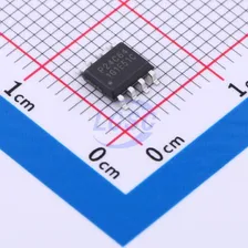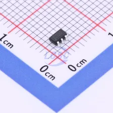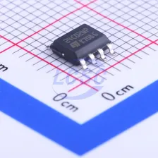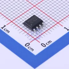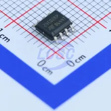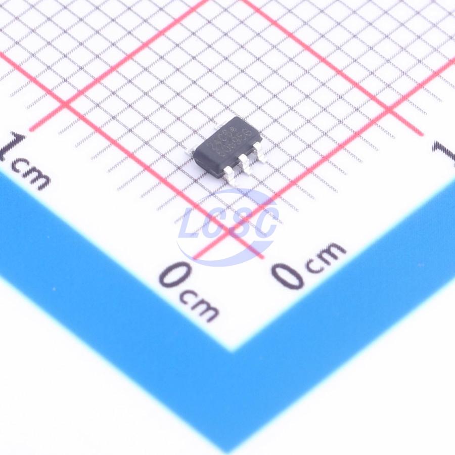
Every Order Guarantee
100% Authentic · 30-Day Return or Replacement · policy
5,285 in stock
#C54582119
Stock & price checked 6 days ago
| Quantity | Unit price | Pack price |
|---|---|---|
| 5+ | ₹20.53 | ₹102.65 |
| 50+ | ₹16.26 | ₹813.00 |
| 150+ | ₹14.43 | ₹2,164.50 |
| 500+ | ₹12.16 | ₹6,080.00 |
| 3,000+ | ₹11.14 | ₹33,420.00 |
| 6,000+ | ₹10.53 | ₹63,180.00 |
5 × ₹20.53
₹102.65
excl. GST
₹121.13 incl. 18% GST
- Dispatch in 7–10 working days
- GST invoice with every order
- Standard pack: 3,000 per reel
ZD24C64A-STGMT
₹102.65 for 5 + GST
Specifications
- Operating Temperature
- -40℃~+105℃
- Features
- Hardware write protection function;Built-in power-on reset (POR);Noise suppression function
- Memory Size
- 64Kbit
- Voltage - Supply
- 1.7V~5.5V;300uA
- Clock Frequency
- 1MHz
- Access Time
- 4500ns
- Data Retention - TDR (Year)
- 100 Years
- Write Cycle Time(tWC)
- 5ms
- Standby Supply Current
- 0.5uA
- Write Cycle Endurance
- 1 million cycles
- Interface
- I2C
Packaging & compliance
- RoHS
- RoHS
- Lifecycle
- Active
- Packaging
- Tape & Reel (TR)
- Standard pack
- 3,000 / Reel
- Sold per
- Piece
- Minimum order
- 5 (multiples of 5)
- Unit weight
- 0.139 g
Overview
The ZD24C64A provides 65,536 bits of serial EEPROM, organized as 8,192 words of 8 bits each. The device offers an additional page called the Identification Page. The Identification Page can be used to store sensitive application parameters that can (later) be permanently locked in read-only mode. The device's cascadable feature allows multiple devices to share a common two-wire bus. The device is optimized for many industrial and commercial applications where low-power and low-voltage operation are essential. The device is available in space-saving 8-lead SOIC, 8-lead TSSOP, 8-pad UDFN, 8-lead PDIP, 5-lead SOT23, and 8-ball UDFN packages. The entire package family operates over a voltage range of 1.7V to 5.5V. If the WP pin is not driven, it is internally pulled down to GND. To ensure reliable operation across various application environments, the pull-down mechanism is intentionally designed to be relatively strong. Once these pins are biased above the trip point of the CMOS input buffer (~0.5×VCC), the pull-down mechanism disengages. It is recommended to connect these pins to a known state whenever possible. The ZD24C64A operates as a slave device and communicates with a master controller using a simple I²C-compatible two-wire digital serial interface. The serial interface consists of only two signal lines: serial clock and serial data. The SCL pin receives the clock signal from the master, while the bidirectional SDA pin receives commands and data from the master and transmits data back to the master. Data is always latched into the ZD24C64A on the rising edge of SCL and is always output from the device on the falling edge of SCL. Both the SCL and SDA pins incorporate spike suppression filters and Schmitt triggers to minimize the effects of input spikes and bus noise. All commands and data are transmitted MSB first. During bus communication, one data bit is transferred per clock cycle; after eight bits of data have been transferred, the receiving device must respond with an ACK or NACK response bit during the ninth clock cycle generated by the master. Therefore, nine clock cycles are required to transfer one byte of data. There are no unused clock cycles during any read or write operation, so no interruptions or gaps are permitted in the data stream during each data byte transfer and during the ACK or NACK clock cycle. During data transfer, data on the SDA pin may only change while SCL is low and must remain stable while SCL is high. If the data on the SDA pin changes while SCL is high, a Start or Stop condition will be generated. Start and Stop conditions are used to initiate and terminate all serial bus communication between the master and slave devices. The number of data bytes transferred between Start and Stop conditions is unlimited and is determined by the master. For the serial bus to be in an idle state, both SCL and SDA pins must simultaneously be at a logic high level. The SDA pin is an open-drain terminal and must therefore be pulled high through an external pull-up resistor. Data on the SDA pin may only change during the low period of SCL. A change in data during the high period of SCL will indicate a Start or Stop condition as defined below. A high-to-low transition on the SDA pin while the SCL pin is at a stable logic 1 state generates a Start condition and causes the device to exit standby mode. The master uses the Start condition to initiate any data transfer sequence; therefore, every command must begin with a Start condition. The device continuously monitors the SDA and SCL pins for a Start condition but will not respond unless one is detected. A low-to-high transition on the SDA pin while the SCL pin is at a stable logic 1 state generates a Stop condition and terminates all communication. Following the Stop condition, the device enters standby low-power mode.
Applications
- Industrial control
- Automotive electronics
- Consumer electronics
- Medical devices
- IoT devices
Key features
- Low-voltage operation: VCC = 1.7V to 5.5V
- Internal organization: 8,192 × 8
- Additional lockable page
- I²C-compatible serial interface
- 100kHz Standard Mode, 1.7V to 5.5V
- 400kHz Fast Mode, 1.7V to 5.5V
- 1MHz Fast Mode Plus, 2.5V to 5.5V
- Schmitt trigger filtered inputs for noise suppression
- Bidirectional data transfer protocol
- Write Protect pin for full array hardware data protection
- Ultra-low active and standby current
- 32-byte page write mode
- Partial page write allowed
- Random and sequential read modes
- Self-timed write cycle, 5ms max
- High reliability: endurance 1,000,000 write cycles; data retention 100 years
- Enhanced ESD/latch-up protection: HBM 4 kV; latch-up capability +/- 200mA
- Green package options
- 8-lead SOIC, 8-lead TSSOP, 8-pad UDFN, 8-lead PDIP, 5-lead SOT23 packages
- Die sales options: wafer form and tape-and-reel
- Identification Page option
Same category