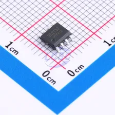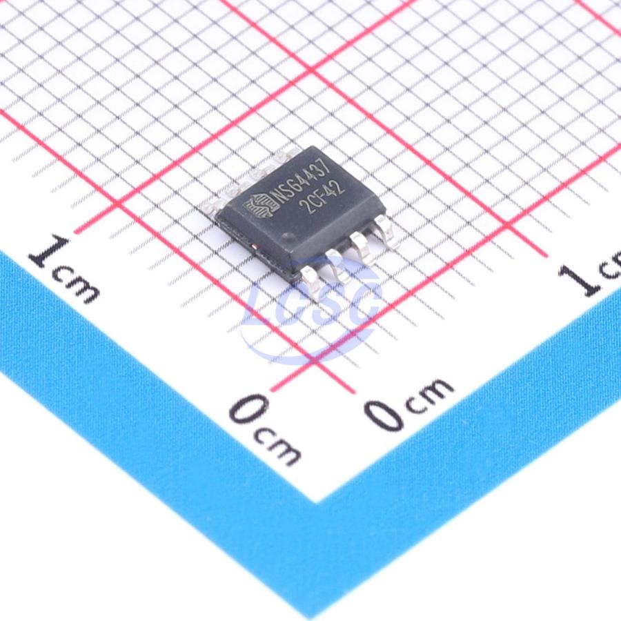
NSG4437
4.5V~20V 2A 2A SOP-8 Gate Drivers
- Manufacturer
- NCE
- Manufacturer part #
- NSG4437
- Store part #
- C53436466
- Package / case
- SOP-8
- Category
- Gate Drivers
- Packaging
- Tape & Reel (TR)
Every Order Guarantee
100% Authentic · 30-Day Return or Replacement · policy
2,800 in stock
#C53436466
Stock & price checked 27 h ago
| Quantity | Unit price | Pack price |
|---|---|---|
| 5+ | ₹39.58 | ₹197.90 |
| 50+ | ₹31.78 | ₹1,589.00 |
| 150+ | ₹28.43 | ₹4,264.50 |
| 500+ | ₹24.26 | ₹12,130.00 |
| 2,500+ | ₹22.41 | ₹56,025.00 |
| 4,000+ | ₹21.29 | ₹85,160.00 |
5 × ₹39.58
₹197.90
excl. GST
₹233.52 incl. 18% GST
- Dispatch in 7–10 working days
- GST invoice with every order
- Standard pack: 4,000 per reel
NSG4437
₹197.90 for 5 + GST
Specifications
- Input Logic Level - Low
- 800mV
- Input Logic Level - High
- 2.4V
- Voltage - Supply
- 4.5V~20V
- Operating Temperature
- -40℃~+125℃
- Driven Configuration
- Low Side
- Current - Output Low(IOL)
- 2A
- Rise Time
- 20ns
- Fall Time
- 20ns
- Current - Output High(IOH)
- 2A
- Load Type
- MOSFET
Packaging & compliance
- RoHS
- RoHS
- Lifecycle
- Active
- Moisture sensitivity
- MSL 3 (168 hours)
- Packaging
- Tape & Reel (TR)
- Standard pack
- 4,000 / Reel
- Sold per
- Piece
- Minimum order
- 5 (multiples of 5)
- Unit weight
- 0.269 g
Overview
The NSG4437 is a driver for power switch families. It features matched rise and fall times when charging and discharging the gates of power switches. The NSG4437 provides high latch-up immunity under any conditions within its rated power and voltage range. When noise spikes of up to 5V (either polarity) appear on the ground pin, the NSG4437 will not be damaged. The NSG4437 can accept up to 500mA of reverse current forced back into its output without damage or logic upset. All terminals are fully protected against up to 2.0kV ESD. The NSG4437 is an ultra-high-speed, high-current power IC driver with matched rise and fall times when charging and discharging the gates of power switches. The NSG4437 provides high latch-up immunity under any conditions within its rated power and voltage range. When noise spikes of up to 5V (either polarity) appear on the ground pin, the NSG4437 will not be damaged. The NSG4437 can accept up to 500mA of reverse current forced back into its output without damage or logic upset. The NSG4437 includes an SD channel shutdown input pin. When the SD pin is logic high, the driver will not trigger any output under any conditions. The NSG4437 includes two independent signal input ports for receiving control signals from the master controller without mutual interference. Both ports are designed with high reliability — even when 500mA of reverse current is forced back into the output, no damage or logic upset will occur. The signal input ports also feature the ability to directly handle voltages down to -10V, ensuring safe operation of the IC even under significant noise waveform interference, thereby improving device stability. It is not recommended to adjust the output waveform by modifying the slope or delay of the input port waveform during design. If adjustment of the rise and fall times on the power stage is required, it is recommended to add external resistors between the output and the power stage. The signal input ports of the NSG4437 have pull-up resistors to GND. It is recommended to short these ports to GND when not in use. The NSG4437 has a built-in 100KΩ pull-down resistor between the SD pin and GND. If the SD function is not used, this pin may be left floating or shorted to GND. In environments with significant EMI noise, it is recommended to connect the EN pin to the VSS pin using a 1nF capacitor placed as close to the EN pin as possible. The NSG4437 output is in phase with the input and can be used to drive either P-type or N-type MOSFETs. Each output port can source or sink peak currents of 2A. Its high-speed, high-current characteristics make it suitable for driving MOSFETs in high-frequency application designs. The high-speed, high-current characteristics of the NSG4437 make it well suited for applications such as high-frequency power supplies. A typical application is where the PWM output stage of a master IC lacks sufficient drive capability for the power stage MOSFETs, requiring a high-power driver IC between the controller and the MOSFETs to drive the gate voltage, ensuring stable MOSFET operation.
Applications
- Switching power supplies, switch-mode converters
- Line drivers
- Pulse transformer driving
- MOSFET and IGBT driving
- Motor control
- Pulse generators
- Power switches
- DC-DC converters
- Class D switching amplifiers
Key features
- Latch-up protection: withstands 0.5A reverse current
- Input logic protection down to -10V
- Low output impedance
- Dual-channel driver on a single chip
- SD simultaneously shuts down both channels, active high
- Output peak current: 2A
- Operating range: 4.5V~25V
- Maximum input voltage up to 25V
- High capacitive load drive capability: switching time <25ns at 1nF load
- Matched rise/fall times
- Wide temperature range: -40℃~125℃
- RoHS-compliant SOP8
Alternatives
Similar parts — check the datasheet before substituting.


Same category